ST7565S
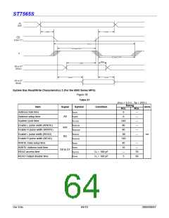
A0
R/W
t
AW6
tAH6
CS1
(CS2="1")
t
CYC6
t
CCLR,tCCLW
E
t
CCHR,tCCHW
t
DH6
t
DS6
D0 to D7
(Write)
tACC6
tOH6
D0 to D7
(Read)
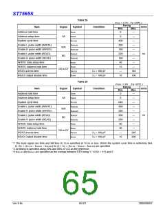
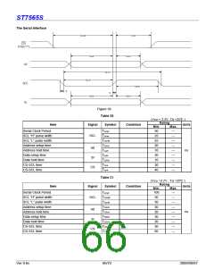
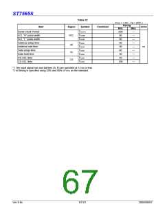
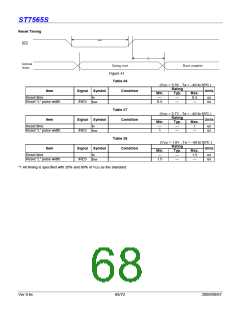
System Bus Read/Write Characteristics 2 (For the 6800 Series MPU)
Figure 38
Table 27
(VDD = 3.3 V , Ta = 25°C )
Rating
Min.
Item
Address hold time
Signal
Symbol
Condition
Units
Max.
0
—
t
t
t
t
t
t
t
t
t
t
t
AH6
A0
Address setup time
0
240
80
80
80
140
40
10
—
—
—
—
—
—
AW6
System cycle time
CYC6
EWLW
EWHW
EWLR
EWHR
DS6
Enable L pulse width (WRITE)
Enable H pulse width (WRITE)
Enable L pulse width (READ)
Enable H pulse width (READ)
WRITE Data setup time
WRITE Address hold time
READ access time
WR
RD
ns
—
—
70
50
DH6
D0 to D7
CL
L
= 100 pF
= 100 pF
ACC6
OH6
READ Output disable time
C
5
Ver 0.6c
64/72
2009/09/07

 SITRONIX [ SITRONIX TECHNOLOGY CO., LTD. ]