ST7565S
ABSOLUTE MAXIMUM RATINGS
Unless otherwise noted, VSS = 0V
Table 17
Parameter
Power Supply Voltage
Symbol
DD
Conditions
–0.3 ~ +5.0
–4.0 ~ -1.8
–18.0 ~ +0.3
Unit
V
V
Power supply voltage (VDD standard)
Power supply voltage (VDD standard)
Power supply voltage (VDD standard)
Input voltage
V
SS2
, VOUT
V
V
5
V
V
1
, V
2, V
3, V
4
V
5
to +0.3
V
V
IN
–0.3 to VDD + 0.3
–0.3 to VDD + 0.3
–40 to +85
V
Output voltage
V
O
V
Operating temperature
TOPR
°C
°C
Storage temperature
TCP
–55 to +100
–55 to +125
TSTR
Bare chip
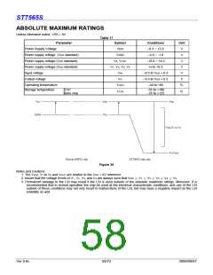
V
CC
V
DD
VDD
GND
VSS
V
SS2,V1 to V4
V5.,VOUT
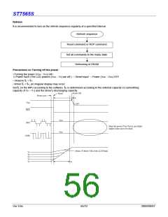
System (MPU) side
ST7565S chip side
Figure 30
Notes and Cautions
1. The VSS2, V
2. Insure that the voltage levels of V
1
to V
5
and VOUT are relative to the VDD = 0V reference.
, V , V , and V are always such that VDD ≧ V1 ≧ V2 ≧ V3 ≧ V4 ≧ V5.
1
2
3
4
3. Permanent damage to the LSI may result if the LSI is used outside of the absolute maximum ratings. Moreover, it is
recommended that in normal operation the chip be used at the electrical characteristic conditions, and use of the LSI
outside of these conditions may not only result in malfunctions of the LSI, but may have a negative impact on the LSI
reliability as well.
Ver 0.6c
58/72
2009/09/07

 SITRONIX [ SITRONIX TECHNOLOGY CO., LTD. ]