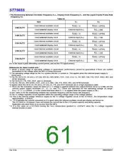
ST7565S
• The Relationship Between Oscillator Frequency fOSC, Display Clock Frequency fCL and the Liquid Crystal Frame Rate
Frequency fFR
Table 23
Item
f
CL
fFR
Used internal oscillator circuit
Used external display clock
Used internal oscillator circuit
Used external display clock
Used internal oscillator circuit
Used external display clock
Used internal oscillator circuit
Used external display clock
Used internal oscillator circuit
Used external display clock
f
OSC / 4
f
f
f
f
f
OSC / (4*65)
CL / 260
OSC / (4*49)
CL / 196
OSC / (8*33)
CL / 264
OSC / (4*55)
CL / 220
OSC / (4*53)
CL / 212
1/65 DUTY
1/49 DUTY
1/33 DUTY
1/55 DUTY
1/53 DUTY
External input (fCL
)
)
)
)
)
f
f
OSC / 4
External input (fCL
f
f
OSC / 8
External input (fCL
f
f
OSC / 4
External input (fCL
f
f
OSC / 4
External input (fCL
f
(fFR is the liquid crystal alternating current period, and not the FR signal period.)
References for items market with *
*1 While a broad range of operating voltages is guaranteed, performance cannot be guaranteed if there are sudden
fluctuations to the voltage while the MPU is being accessed.
*2 The operating voltage range for the VDD system and the V
being used.
5 system is. This applies when the external power supply is
*3 The A0, D0 to D5, D6 (SCL), D7 (SI), /RD (E), /WR (R/W), /CS1, CS2, CLS, CL, FR, M/S, C86, P/S, /DOF, /RES, IRS, and
/HPM terminals.
*4 The D0 to D7, FR, FRS, /DOF, and CL terminals.
*5 The A0, /RD (E), /WR (R/W), /CS1, CS2, CLS, M/S, C86, P/S, /RES, IRS, and /HPM terminals.
*6 Applies when the D0 to D5, D6 (SCL), D7 (SI), CL, FR, and /DOF terminals are in a high impedance state.
*7 These are the resistance values for when a 0.1 V voltage is applied between the output terminal SEGn or COMn and the
various power supply terminals (V
ON = 0.1 V /ΔI (Where ΔI is the current that flows when 0.1 V is applied while the power supply is ON.)
*8 See Table 23 for the relationship between the oscillator frequency and the frame rate frequency.
*9 The V voltage regulator circuit regulates within the operating voltage range of the voltage follower.
1, V2, V3, and V4). These are specified for the operating voltage (3) range.
R
5
*10 This is the internal voltage reference supply for the V
approximately –0.05%/°C.
5 voltage regulator circuit. In the ST7565S , the temperature range
*11, 12 It indicates the current consumed on ICs alone when the internal oscillator circuit and display are turned on.
The ST7565S is 1/9 biased. Does not include the current due to the LCD panel capacity and wiring capacity.
Applicable only when there is no access from the MPU.
*12 It is the value on a ST7565S having the VREG temperature gradient is –0.05%/°C when the V
internal resistor is used.
5 voltage regulator
Ver 0.6c
61/72
2009/09/07

 SITRONIX [ SITRONIX TECHNOLOGY CO., LTD. ]