SiI 1161 PanelLink Receiver
Data Sheet
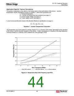
Application-Specific Thermal Calculations
The junction temperature of the silicon is the limiting factor to the performance of this device. Junction
temperature may be calculated as shown in Equation 1, where the input factors are:
TA Ambient temperature.
ΘJA Junction-to-Ambient thermal resistance (see page 3).
VCC Power supply voltage (see page 3).
ICC Power supply current (see page 4).
TJ must not exceed the limit shown in the Absolute Maximum specifications on page 3
T
J
= T +θJA ×VCC × ICC
A
Equation 1. Junction Temperature Calculation
The temperature rise, from ambient to junction (Figure 31), is a function of the power demanded by the operation
of the device, and the thermal resistance of the device. Power consumption is a function of the pixel frequency.
Thermal resistance is a function of the soldered use of the package’s ePad.
70.00
60.00
50.00
40.00
30.00
20.00
10.00
0.00
25
40
65
108
135
165
RxC Frequency (MHz)
ePad 100% soldered
ePad 20% soldered
ePad unsoldered
Figure 31. Temperature Rise with Frequency and ePad
SiI-DS-0096-D
40

 SILICONIMAGE [ Silicon image ]