SiI 1160 PanelLink Transmitter
Data Sheet
Pin Descriptions
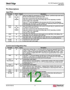
Input Pins
Pin Name
DIE23-
DIE0
Pin #
Type
Description
See
In
Input Even Data[23:0] corresponds to 24-bit pixel data for 1-pixel/clock input mode and to
the first 24-bit pixel data for 2-pixels/clock mode.
SiI 1160
Pin
Input data is synchronized with Input data clock (IDCK).
Diagram
Data can be latched on the rising of the falling edge of IDCK depending on whether
EDGE is high or low, respectively.
Refer to TFT Panel Data Mapping in this document and DSTN Panel Data Mapping
application note (SiI-AN-0007-A), which tabulates the relationship between the input data
to the transmitter and output data from the Receiver
DIO23-
DIO0
See
In
Input Odd Data[23:0] corresponds to the second 24-bit pixel data for 2-pixels/clock mode.
Tie all pins to low when not in use.
SiI 1160
Pin
Input data is synchronized with Input data clock (IDCK).
Diagram
Data can be latched on the rising of the falling edge of IDCK depending on whether
EDGE is high or low, respectively.
Dual Link is not supported.
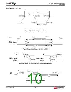
IDCK
DE
80
78
In
In
Input Data Clock. Input data and control signals can be valid either on the falling or the
rising edge of IDCK as selected by the EDGE pin.
Input Data Enable. This signal qualifies the active data area. DE is always required by the
transmitter and must be high during active display time and low during blanking time.
HSYNC
VSYNC
76
77
In
In
Horizontal Sync input control signal.
Vertical Sync input control signal.
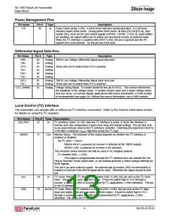
Control and Configuration Pins
Pin Name
Pin #
Type
Description
EDGE
24
In
Data/Control Latching Edge. A LOW level indicates that all input signals(DIE/DIO[23:0],
HSYNC, VSYNC, DE and CTL[3:1] are latched on the falling edge of IDCK, while a HIGH
level(3.3V) indicates that all input signals are latched on the rising edge of IDCK. When
the I2C interface is enabled (ISEL/RST=LOW), this pin is ignored and the EDGE register
bit is used instead.
PIXS
25
84
In
In
Pixel Select. A LOW level indicates one pixel (up to 24-bits) per clock mode using
DIE[23:0]. A HIGH level (3.3V) indicates two pixels (up to 48-bits) per clock mode using
DIE[23:0] for the first pixel and DIO[23:0] for the second pixel.
CTL1
General Input control signal 1.
SS_CLK_IN
Spread Spectrum Clock Input (future). A planned future variation of this device will allow
a spread spectrum version of SS_CLK_OUT to be driven into this pin, at which time pin
29 will become CTL1.
CTL2
83
In
General Input control signal 2.
SS_CLK_OUT
Out Spread Spectrum Clock Output (future). A planned future variation of this device will
allow a clock to be driven out of this pin for conditioning by a spread spectrum device, at
which time pin 28 will become CTL2.
CTL3
RSVD
82
27
In
In
General Input control signal 3.
Reserved. Must be tied HIGH for normal operation.
SS_EN#
Spread Spectrum Enable. A planned future variation of this device will use this pin to
enable pins 83 and 84 to handle spread spectrum clock.
Low = Spread Spectrum feature enabled on pins 83 and 84
High = Pins 83 and 84 are CTL2 and CTL1 outputs (default)
SiI-DS-0126-B
8

 SILICONIMAGE [ Silicon image ]