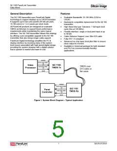
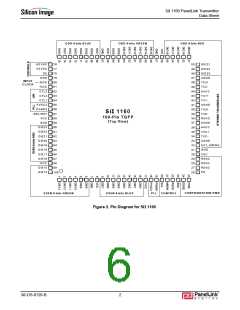
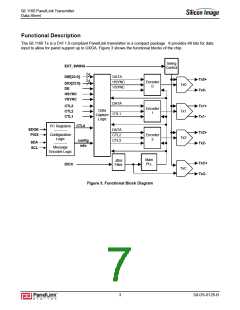
SiI 1160 PanelLink Transmitter
Data Sheet
DC Specifications
Under normal operating conditions, with REXT_SWING = 510Ω and using source termination, unless otherwise
specified.
Symbol
Parameter
Conditions
Min
Typ
Max Units
VOD
Differential Voltage
RLOAD = 50Ω
Single ended peak to peak
amplitude
510
550
590
mV
V
VDOH
IDOS
Differential High-level Output
Voltage1
AVCC
Differential Output Short
VOUT = 0 V
5
5
µA
mA
mA
Circuit Current1
IPD
Power-down Current2
ICCT
Transmitter Supply Current
IDCK= 165 MHz, two pixel per
clock mode
IVCC = VCC, Worst Case Pattern3
140
200
Notes
1. Guaranteed by design.
2. Assumes all inputs to the transmitter are not toggling.
3. The Worst Case Pattern consists of a black and white checkerboard pattern, each checker one pixel wide.
AC Specifications
Under normal operating conditions with source termination and the recommended REXT_SWING value unless
otherwise specified.
Symbol
TCIP
Parameter
IDCK Period, 1 Pixel/Clock
Conditions
Min
6
Max
40
Units
ns
FCIP
IDCK Frequency, 1 Pixel/Clock
25
12
12
2
165
80
MHz
ns
TCIP
IDCK Period, 2 Pixels/Clock
FCIP
IDCK Frequency, 2 Pixels/Clock
IDCK High Time at 165MHz
81
MHz
ns
TCIH
TCIL
IDCK Low Time at 165MHz
2
ns
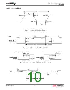
TSIDF
Data, DE, VSYNC, HSYNC, and CTL[3:1]
Setup Time to IDCK falling edge
Data, DE, VSYNC, HSYNC, and CTL[3:1]
Hold Time from IDCK falling edge
Data, DE, VSYNC, HSYNC, and CTL[3:1]
Setup Time to IDCK rising edge
Data, DE, VSYNC, HSYNC, and CTL[3:1]
Hold Time from IDCK rising edge
EDGE = 0
EDGE = 0
EDGE = 1
EDGE = 1
1.5
ns
THIDF
TSIDR
THIDR
TDDF
1.5
1.5
1.5
ns
ns
ns
ns
VSYNC, HSYNC, and CTL[3:1] Delay from DE falling
TCIP
TCIP
edge1
TDDR
THDE
VSYNC, HSYNC, and CTL[3:1] Delay to DE rising edge1
DE high time1
ns
ns
ns
ns
µs
8191TCIP
1000
TLDE
DE low time1
128TCIP
50
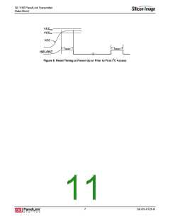
TI2CDVD
TRESET
SDA Data Valid Delay from SCL high to low transition
ISEL/RST Signal High Time required for valid I2C reset
CL = 400pf
Notes
1. Guaranteed by design.
2. All TMDS signaling is guaranteed to meet the DVI 1.0 specifications.
3. All Standard mode I2C (100kHz and 400kHz) timing requirements are guaranteed by design.
5
SiI-DS-0126-B

 SILICONIMAGE [ Silicon image ]