SiI 1160 PanelLink Transmitter
Data Sheet
Electrical Specifications
Absolute Maximum Conditions
Symbol
VCC
VI
Parameter
Supply Voltage 3.3V
Min
-0.3
-0.3
-0.3
Typ
Max
4.0
Units
V
1
Input Voltage
VCC+ 0.3
VCC+ 0.3
125
V
2
VO
Tj
Input Voltage
V
Junction Temperature (with power applied)
Storage Temperature
°C
°C
TSTG
-65
150
Note
1. Permanent device damage may occur if absolute maximum conditions are exceeded.
2. Functional operation should be restricted to the conditions described under normal operating conditions.
Normal Operating Conditions
Symbol
VCC
Parameter
Min Typ Max Units
Supply Voltage
3.0
3.3
3.6
100
70
V
VCCN
TA
Supply Voltage Noise
mVP-P
°C
Ambient Temperature (with power applied)
Thermal Resistance (junction to ambient)1
0
25
θJA
53
°C/W
Note
1. Airflow at 0m/s.
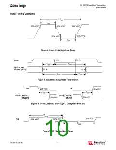
Digital I/O Specifications
Under normal operating conditions unless otherwise specified.
Symbol
VIH
Parameter
High-level Input Voltage
Low-level Input Voltage
High-level Input Voltage
Low-level Input Voltage
Input Clamp Voltage1
Input Clamp Voltage1
Input Clamp Voltage1
Input Clamp Voltage1
Input Leakage Current
Conditions
Min Typ
2
Max
Units
V
V
VIL
0.8
VOH
2.4
V
VOL
0.4
V
VCINL
VCIPL
VCONL
VCOPL
IOL
ICL = -18mA
GND -0.8
IVCC + 0.8
GND -0.8
V
ICL = 18mA
V
ICL = -18mA
ICL = 18mA
V
OVCC + 0.8
10
V
High Impedance
-10
µA
Note
1. Guaranteed by design. Voltage undershoot or overshoot cannot exceed absolute maximum conditions for a pulse of
greater than 3 ns or one third of the clock cycle.
SiI-DS-0126-B
4

 SILICONIMAGE [ Silicon image ]