C8051F52x-53x
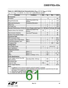
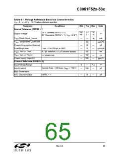
Table 6.1. Voltage Reference Electrical Characteristics
VDD = 2.1 V; –40 to +125 °C unless otherwise specified.
Parameter
Conditions
Min Typ Max
Units
Internal Reference (REFBE = 1)
TBD 1.5 TBD
TBD 2.2 TBD
25 °C ambient (REFLV = 0)
25 °C ambient (REFLV = 1), V = 2.6 V
Output Voltage
V
DD
V
V
Short-Circuit Current
—
—
TBD
mA
REF
REF
Temperature Coefficient
—
—
—
—
33
30
—
—
—
—
ppm/°C
µA
Power Consumption (Internal)
Load Regulation
Load = 0 to 200 µA to GND
4.7 µF tantalum, 0.1 µF ceramic bypass
no bypass cap
10
ppm/µA
ms
V
V
Turn-on Time 1
Turn-on Time 2
TBD
REF
REF
—
—
TBD
TBD
—
—
µs
Power Supply Rejection
ppm/V
External Reference (REFBE = 0)
V
Input Voltage Range
0
—
V
DD
Sample Rate = 200 ksps; V
= TBD V
Input Current
—
TBD
—
µA
REF
Bias Generators
ADC Bias Generator
BIASE = ‘1’
—
30
—
µA
Rev. 0.3
65

 SILICON [ SILICON ]