C8051F52x-53x
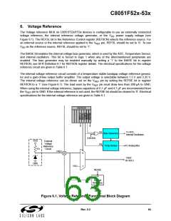
6. Voltage Reference
The Voltage reference MUX on C8051F52x/F53x devices is configurable to use an externally connected
voltage reference, the internal reference voltage generator, or the V power supply voltage (see
DD
Figure 6.1). The REFSL bit in the Reference Control register (REF0CN) selects the reference source. For
an external source or the internal reference applied to the V pin, REFSL should be set to ‘0’. To use
REF
V
as the reference source, REFSL should be set to ‘1’.
DD
The BIASE bit enables the internal voltage bias generator, which is used by the ADC, Temperature Sensor,
and internal oscillators. This bit is forced to logic 1 when any of the aforementioned peripherals are
enabled. The bias generator may be enabled manually by writing a ‘1’ to the BIASE bit in register
REF0CN; see SFR Definition 6.1 for REF0CN register details. The electrical specifications for the voltage
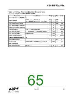
reference circuit are given in Table 6.1.
The internal voltage reference circuit consists of a temperature stable bandgap voltage reference genera-
tor and a gain-of-two output buffer amplifier. The output voltage is selectable between 1.5 V and 2.25 V.
The internal voltage reference can be driven out on the V
pin by setting the REFBE bit in register
REF
REF0CN to a ‘1’ (see Figure 6.1). The load seen by the V
pin must draw less than 200 µA to GND.
REF
When using the internal voltage reference, bypass capacitors of 0.1 µF and 4.7 µF are recommended from
the V pin to GND. If the internal reference is not used, the REFBE bit should be cleared to ‘0’. Electrical
REF
specifications for the internal voltage reference are given in Table 6.1.
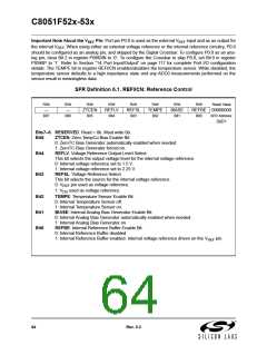
REF0CN
To ADC,
Internal Oscillators
EN
Bias Generator
IOSCEN
VDD
External
Voltage
EN
Temp Sensor
To Analog Mux
Reference
Circuit
R1
VREF
0
1
VREF
(to ADC)
GND
VDD
REFBE
EN
Internal
Reference
REFLV
Figure 6.1. Voltage Reference Functional Block Diagram
Rev. 0.3
63

 SILICON [ SILICON ]