C8051F52x-53x
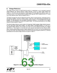
Important Note About the V
Pin: Port pin P0.0 is used as the external V
input and as an output for
REF
REF
the internal V
. When using either an external voltage reference or the internal reference circuitry, P0.0
REF
should be configured as an analog pin, and skipped by the Digital Crossbar. To configure P0.0 as an ana-
log pin, clear Bit 2 in register P0MDIN to ‘0’. To configure the Crossbar to skip P0.0, set Bit 0 in register
P0SKIP to ‘1’. Refer to Section “14. Port Input/Output” on page 117 for complete Port I/O configuration
details. The TEMPE bit in register REF0CN enables/disables the temperature sensor. While disabled, the
temperature sensor defaults to a high impedance state and any ADC0 measurements performed on the
sensor result in meaningless data.
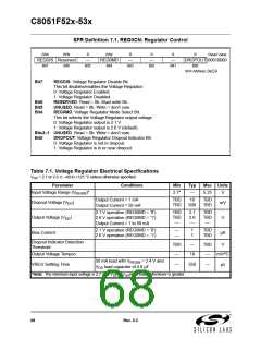
SFR Definition 6.1. REF0CN: Reference Control
R/W
—
R/W
—
R/W
ZTCEN
Bit5
R/W
REFLV
Bit4
R/W
REFSL
Bit3
R/W
TEMPE
Bit2
R/W
BIASE
Bit1
R/W
Reset Value
REFBE 00000000
Bit0
Bit7
Bit6
SFR Address:
0xD1
Bits7–6: RESERVED. Read = 0b. Must write 0b.
Bit5:
ZTCEN: Zero-TempCo Bias Enable Bit.
0: ZeroTC Bias Generator automatically enabled when needed.
1: ZeroTC Bias Generator forced on.
Bit4:
REFLV: Voltage Reference Output Level Select.
This bit selects the output voltage level for the internal voltage reference.
0: Internal voltage reference set to 1.5 V.
1: Internal voltage reference set to 2.25 V.
Bit3:
REFSL: Voltage Reference Select.
This bit selects the source for the internal voltage reference.
0: V
pin used as voltage reference.
REF
1: V used as voltage reference.
DD
Bit2:
Bit1:
Bit0:
TEMPE: Temperature Sensor Enable Bit.
0: Internal Temperature Sensor off.
1: Internal Temperature Sensor on.
BIASE: Internal Analog Bias Generator Enable Bit.
0: Internal Analog Bias Generator automatically enabled when needed.
1: Internal Analog Bias Generator on.
REFBE: Internal Reference Buffer Enable Bit.
0: Internal Reference Buffer disabled.
1: Internal Reference Buffer enabled. Internal voltage reference driven on the V
pin.
REF
64
Rev. 0.3

 SILICON [ SILICON ]