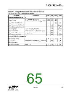
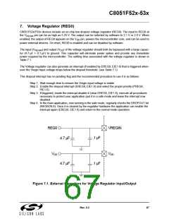
C8051F52x-53x
8. Comparator
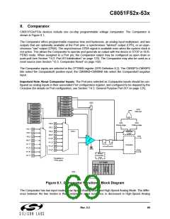
C8051F52x/F53x devices include one on-chip programmable voltage comparator. The Comparator is
shown in Figure 8.1;
The Comparator offers programmable response time and hysteresis, an analog input multiplexer, and two
outputs that are optionally available at the Port pins: a synchronous “latched” output (CP0), or an asyn-
chronous “raw” output (CP0A). The asynchronous CP0A signal is available even when the system clock is
not active. This allows the Comparator to operate and generate an output with the device in STOP or SUS-
PEND mode. When assigned to a Port pin, the Comparator output may be configured as open drain or
push-pull (see Section “14.2. Port I/O Initialization” on page 123). The Comparator may also be used as a
reset source (see Section “12.5. Comparator Reset” on page 102).
The Comparator inputs are selected in the CPT0MX register (SFR Definition 8.2). The CMX0P3–CMX0P0
bits select the Comparator0 positive input; the CMX0N3–CMX0N0 bits select the Comparator0 negative
input.
Important Note About Comparator Inputs: The Port pins selected as Comparator inputs should be con-
figured as analog inputs in their associated Port configuration register, and configured to be skipped by the
Crossbar (for details on Port configuration, see Section “14.3. General Purpose Port I/O” on page 125).
CP0EN
CP0OUT
CP0RIF
CP0FIF
VDD
CMX0N3
CMX0N2
CMX0N1
CMX0N0
CMX0P3
CMX0P2
CMX0P1
CMX0P0
CP0HYP1
CP0HYP0
CP0HYN1
CP0HYN0
CP0
Interrupt
CP0
Rising-edge
CP0
Falling-edge
P0.0
P0.2
P0.4
P0.1
P0.3
CP0 +
Interrupt
Logic
P0.6*
P1.0*
CP0
P0.5
+
-
SET
CLR
SET
CLR
D
Q
Q
D
Q
Q
P0.7*
P1.1*
P1.3*
P1.5*
P1.7*
P1.2*
P1.4*
P1.6*
Crossbar
(SYNCHRONIZER)
GND
CP0A
Reset
Decision
Tree
*Available in
‘F53x parts
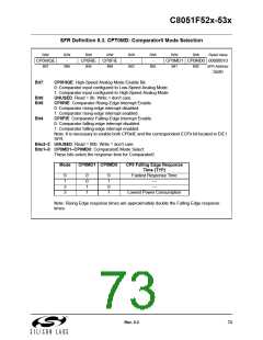
CPT0MD
CP0 -
Figure 8.1. Comparator Functional Block Diagram
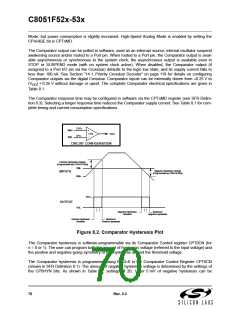
The Comparator has two input modes: Low-Speed Analog Mode and High-Speed Analog Mode. The differ-
ence between the two modes is that Comparator input resistance is decreased in High-Speed Analog
Rev. 0.3
69

 SILICON [ SILICON ]