C8051F52x-53x
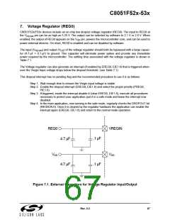
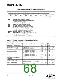
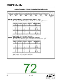
SFR Definition 7.1. REG0CN: Regulator Control
R/W
R/W
R
R/W
REG0MD
Bit4
R
R
R
R
Reset Value
REGDIS Reserved
—
Bit5
—
Bit3
—
Bit2
—
Bit1
DROPOUT 00010000
Bit7
Bit6
Bit0
SFR Address:
0xC9
Bit7:
REGDIS: Voltage Regulator Disable Bit.
This bit disables/enables the Voltage Regulator.
0: Voltage Regulator Enabled.
1: Voltage Regulator Disabled.
Bit6:
Bit5:
Bit4:
RESERVED. Read = 0b. Must write 0b.
UNUSED. Read = 0b. Write = don’t care.
REG0MD: Voltage Regulator Mode Select Bit.
This bit selects the Voltage Regulator output voltage.
0: Voltage Regulator output is 2.1 V.
1: Voltage Regulator output is 2.6 V (default).
Bits3–1: UNUSED. Read = 0b. Write = don’t care.
Bit0:
DROPOUT: Voltage Regulator Dropout Indicator Bit.
0: Voltage Regulator is not in dropout.
1: Voltage Regulator is in or near dropout.
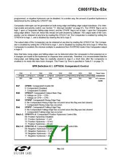
Table 7.1. Voltage Regulator Electrical Specifications
VDD = 2.1 or 2.6 V; –40 to +125 °C unless otherwise specified.
Parameter
Conditions
Min
Typ
Max Units
Input Voltage Range (V
)*
2.7*
—
5.25
V
REGIN
Output Current = 1 mA
Output Current = 50 mA
TBD
TBD
10
500
TBD
TBD
Dropout Voltage (V
)
mV
DO
2.1 V operation (REG0MD = ‘0’)
2.6 V operation (REG0MD = ‘1’)
Output Current = 1 to 50 mA
TBD
TBD
—
2.1
2.6
—
TBD
TBD
—
Output Voltage (V
)
V
DD
2.1 V operation (REG0MD = ‘0’)
2.6 V operation (REG0MD = ‘1’)
—
—
1
1
TBD
TBD
Bias Current
µA
Dropout Indicator Detection
Threshold
TBD
—
—
TBD
—
V
Output Voltage Tempco
18
mV/ºC
50 mA load with V
= 2.4 V and
REGIN
VREG Settling Time
—
250
—
µs
V
load capacitor of 4.8 µF
DD
*Note: The minimum input voltage is 2.7 V or V
+ VDO(max load), whichever is greater.
DD
68
Rev. 0.3

 SILICON [ SILICON ]