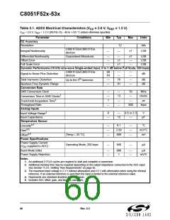
C8051F52x-53x
Table 5.1. ADC0 Electrical Characteristics (V = 2.6 V, V
= 1.5 V)
DD
VDD = 2.6 V, VREF = 1.5 V (REFSL=0), –40 to +125 °C unless otherwise specified.
REF
Parameter
DC Accuracy
Conditions
Min
Typ
Max
Units
Resolution
12
—
bits
C8051F52x/C8051F53x
devices
Integral Nonlinearity
—
±1
LSB
Differential Nonlinearity
Offset Error
Guaranteed Monotonic
—
—
—
—
±1
±1
±1
—
—
LSB
LSB
LSB
Full Scale Error
Dynamic Performance (10 kHz sine-wave Single-ended input, 0 to 1 dB below Full Scale, 200 ksps)
C8051F52x/C8051F53x
devices
68
64
—
—
—
—
Signal-to-Noise Plus Distortion
dB
th
Total Harmonic Distortion
Spurious-Free Dynamic Range
Conversion Rate
—
—
76
91
—
—
dB
dB
Up to the 5 harmonic
SAR Conversion Clock
—
—
1
—
13
—
—
10
—
MHz
clocks
µs
1
Conversion Time in SAR Clocks
2
—
Track/Hold Acquisition Time
Throughput Rate
—
200
ksps
Analog Inputs
3
0
—
4.6 or 2.3
—
V
Input Voltage Range
Input Capacitance
—
12
pF
Temperature Sensor
4,5
—
—
—
0.1
2.89
888
—
—
—
°C
mV/°C
mV
Linearity
4,5
Gain
4,5
(Temp = 25 °C)
Offset
Power Specifications
Power Supply Current
Operating Mode, 200 ksps
—
840
—
µA
(V supplied to ADC)
DD
Burst Mode (Idle)
Power Supply Rejection
Notes:
—
—
880
1
—
—
µA
mV/V
1. An additional 2 FCLK cycles are required to start and complete a conversion.
2. Additional tracking time may be required depending on the output impedance connected to the ADC input.
See Section “5.3.6. Settling Time Requirements” on page 48.
3. The maximum input voltage is 2.3 V without attenuation and 4.6 V with attenuation when using the internal
reference. If an external reference is used then the input is limited to the external reference value.
4. Represents one standard deviation from the mean.
5. Includes ADC offset, gain, and linearity variations.
60
Rev. 0.3

 SILICON [ SILICON ]