C8051F52x-53x
4. Pinout and Package Definitions
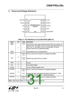
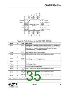
RST/C2CK
P0.0/VREF
GND
1
2
3
4
5
10
9
P0.1/C2D
P0.2/XTAL1
P0.3/XTAL2
P0.4/TX
C8051F520/1/3/4/6/7
Top View
8
VDD
7
VREGIN
6
P0.5/CNVSTR/RX
GND
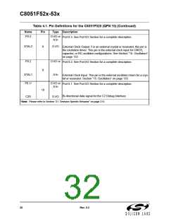
Table 4.1. Pin Definitions for the C8051F520 (QFN 10)
Name
Pin
Type Description
D I/O
Device Reset. Open-drain output of internal POR or V monitor. An
RST/
DD
external source can initiate a system reset by driving this pin low for at
least 15 µs. A 1 kΩ pullup to V is recommended. See Reset
Sources Section for a complete description.
DD
1
2
D I/O
C2CK
P0.0/
Clock signal for the C2 Debug Interface.
D I/O or
A In
Port 0.0. See Port I/O Section for a complete description.
V
A O or
D In
REF
External V
Ground.
Input. See V
Section.
REF
REF
GND
3
4
5
V
Core Supply Voltage.
DD
V
On-Chip Voltage Regulator Input.
REGIN
P0.5/RX*/
D I/O or
A In
Port 0.5. See Port I/O Section for a complete description.
6
External Converter start input for the ADC0, see Section “5. 12-Bit
ADC (ADC0)” on page 41 for a complete description.
CNVSTR
P0.4/TX*
D In
D I/O or
A In
Port 0.4. See Port I/O Section for a complete description.
7
*Note: Please refer to Section “21. Revision Specific Behavior” on page 215.
Rev. 0.3
31

 SILICON [ SILICON ]