C8051F52x-53x
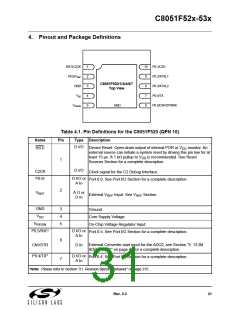
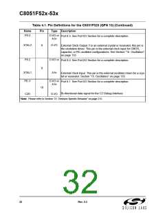
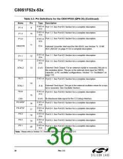
Table 4.1. Pin Definitions for the C8051F520 (QFN 10) (Continued)
Name
Pin
Type Description
P0.3
D I/O or
A In
Port 0.3. See Port I/O Section for a complete description.
XTAL2
P0.2
D I/O
8
External Clock Output. For an external crystal or resonator, this pin is
the excitation driver. This pin is the external clock input for CMOS,
capacitor, or RC oscillator configurations. See Section “15. Oscillators”
on page 133.
D I/O or
A In
Port 0.2. See Port I/O Section for a complete description.
9
XTAL1
P0.1/
External Clock Input. This pin is the external oscillator return for a crys-
tal or resonator. Section “15. Oscillators” on page 133.
D I/O or
A In
Port 0.1. See Port I/O Section for a complete description.
10
Bi-directional data signal for the C2 Debug Interface
C2D
D I/O
*Note: Please refer to Section “21. Revision Specific Behavior” on page 215.
32
Rev. 0.3

 SILICON [ SILICON ]