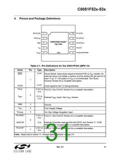
C8051F52x-53x
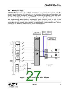
1.8. Port Input/Output
C8051F52x/F53x devices include up to 16 I/O pins. Port pins are organized as two byte-wide ports. The
port pins behave like typical 8051 ports with a few enhancements. Each port pin can be configured as a
digital or analog I/O pin. Pins selected as digital I/O can be configured for push-pull or open-drain opera-
tion. The “weak pullups” that are fixed on typical 8051 devices may be globally disabled to save power.
The Digital Crossbar allows mapping of internal digital system resources to port I/O pins. On-chip
counter/timers, serial buses, hardware interrupts, and other digital signals can be configured to appear on
the port pins using the Crossbar control registers. This allows the user to select the exact mix of general-
purpose port I/O, digital, and analog resources needed for the application.
P0MASK, P0MATCH
P1MASK, P1MATCH
Registers
XBR0, XBR1,
PnSKIP Registers
PnMDOUT,
PnMDIN Registers
Priority
Decoder
2
4
UART
SPI
Highest
Priority
2
2
LIN
Digital
Crossbar
P0.0
P0.7
P1.0*
P1.7*
P0
I/O
Cells
8
8
CP0
Outputs
P1
I/O
Cells
SYSCLK
PCA
7
2
Lowest
Priority
T0, T1
8
8
*Available in ‘F53x
devices
(P0.0-P0.7)
(P1.0-P1.7*)
P0
P1
Figure 1.7. Port I/O Functional Block Diagram
Rev. 0.3
27

 SILICON [ SILICON ]