C8051F52x-53x
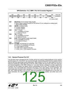
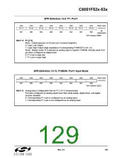
SFR Definition 14.9. P1: Port1
R/W
R/W
R/W
R/W
R/W
R/W
R/W
R/W
Reset Value
P1.7
P1.6
P1.5
P1.4
P1.3
P1.2
P1.1
P1.0
11111111
Bit
Bit7
Bit6
Bit5
Bit4
Bit3
Bit2
Bit1
Bit0
Addressable
SFR Address:
0x90
Bits7–0: P1.[7:0]
Write - Output appears on I/O pins per Crossbar Registers.
0: Logic Low Output.
1: Logic High Output (high impedance if corresponding P1MDOUT.n bit = 0).
Read - Always reads ‘0’ if selected as analog input in register P1MDIN. Directly reads Port
pin when configured as digital input.
0: P1.n pin is logic low.
1: P1.n pin is logic high.
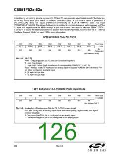
SFR Definition 14.10. P1MDIN: Port1 Input Mode
R/W
Bit7
R/W
Bit6
R/W
Bit5
R/W
Bit4
R/W
Bit3
R/W
Bit2
R/W
Bit1
R/W
Reset Value
11111111
Bit0
SFR Address:
0xF2
Bits7–0: Analog Input Configuration Bits for P1.7–P1.0 (respectively).
Port pins configured as analog inputs have their weak pullup, digital driver, and digital
receiver disabled.
0: Corresponding P1.n pin is configured as an analog input.
1: Corresponding P1.n pin is not configured as an analog input.
Rev. 0.3
129

 SILICON [ SILICON ]