C8051F52x-53x
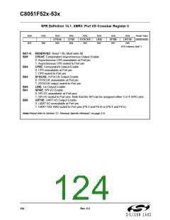
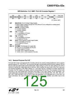
SFR Definition 14.2. XBR1: Port I/O Crossbar Register 1
R/W
R/W
R/W
T1E
Bit5
R/W
T0E
Bit4
R/W
ECIE
Bit3
R/W
—
R/W
R/W
Reset Value
WEAKPUD XBARE
PCA0ME
Bit1
00000000
Bit7
Bit6
Bit2
Bit0
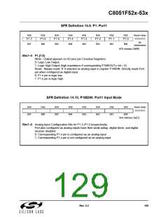
SFR Address:
0xE2
Bit7:
WEAKPUD: Port I/O Weak Pullup Disable.
0: Weak Pullups enabled (except for Ports whose I/O are configured as analog input).
1: Weak Pullups disabled.
XBARE: Crossbar Enable.
0: Crossbar disabled.
1: Crossbar enabled.
T1E: T1 Enable
0: T1 unavailable at Port pin.
1: T1 routed to Port pin.
T0E: T0 Enable
0: T0 unavailable at Port pin.
1: T0 routed to Port pin.
ECIE: PCA0 External Counter Input Enable
0: ECI unavailable at Port pin.
1: ECI routed to Port pin.
Bit6:
Bit5:
Bit4:
Bit3:
Bit2:
Reserved.
Bits1–0: PCA0ME: PCA Module I/O Enable Bits.
00: All PCA I/O unavailable at Port pins.
01: CEX0 routed to Port pin.
10: CEX0, CEX1 routed to Port pins.
11: CEX0, CEX1, CEX2 routed to Port pins.
14.3. General Purpose Port I/O
Port pins that remain unassigned by the Crossbar and are not used by analog peripherals can be used for
general purpose I/O. Ports P0–P1 are accessed through corresponding special function registers (SFRs)
that are both byte addressable and bit addressable. When writing to a Port, the value written to the SFR is
latched to maintain the output data value at each pin. When reading, the logic levels of the Port's input pins
are returned regardless of the XBRn settings (i.e., even when the pin is assigned to another signal by the
Crossbar, the Port register can always read its corresponding Port I/O pin). The exception to this is the
execution of the read-modify-write instructions that target a Port Latch register as the destination. The
read-modify-write instructions when operating on a Port SFR are the following: ANL, ORL, XRL, JBC, CPL,
INC, DEC, DJNZ and MOV, CLR or SETB, when the destination is an individual bit in a Port SFR. For
these instructions, the value of the latch register (not the pin) is read, modified, and written back to the
SFR.
Rev. 0.3
125

 SILICON [ SILICON ]