C8051F52x-53x
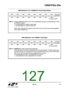
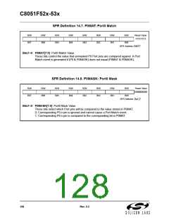
In addition to performing general purpose I/O, P0 and P1 can generate a port match event if the logic lev-
els of the Port’s input pins match a software controlled value. A port match event is generated if
(P0 & P0MASK) does not equal (P0MATCH & P0MASK) or if (P1 & P1MASK) does not equal
(P1MATCH & P1MASK). This allows Software to be notified if a certain change or pattern occurs on P0 or
P1 input pins regardless of the XBRn settings. A port match event can cause an interrupt if EMAT (EIE2.1)
is set to '1' or cause the internal oscillator to awaken from SUSPEND mode. See Section “15.1.1. Internal
Oscillator Suspend Mode” on page 134 for more information.
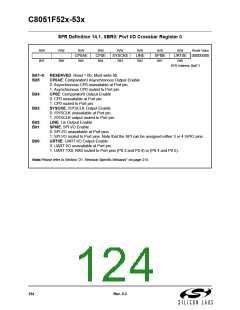
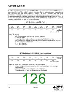
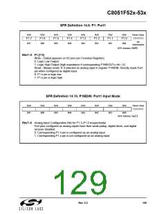
SFR Definition 14.3. P0: Port0
R/W
R/W
R/W
R/W
R/W
R/W
R/W
R/W
Reset Value
P0.7
P0.6
P0.5
P0.4
P0.3
P0.2
P0.1
P0.0
11111111
Bit
Bit7
Bit6
Bit5
Bit4
Bit3
Bit2
Bit1
Bit0
Addressable
SFR Address:
0x80
Bits7–0: P0.[7:0]
Write - Output appears on I/O pins per Crossbar Registers.
0: Logic Low Output.
1: Logic High Output (high impedance if corresponding P0MDOUT.n bit = 0).
Read - Always reads ‘0’ if selected as analog input in register P0MDIN. Directly reads Port
pin when configured as digital input.
0: P0.n pin is logic low.
1: P0.n pin is logic high.
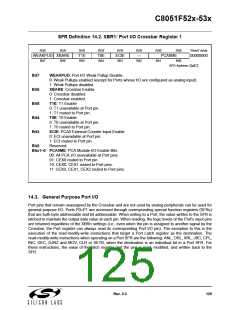
SFR Definition 14.4. P0MDIN: Port0 Input Mode
R/W
Bit7
R/W
Bit6
R/W
Bit5
R/W
Bit4
R/W
Bit3
R/W
Bit2
R/W
Bit1
R/W
Reset Value
11111111
Bit0
SFR Address:
0xF1
Bits7–0: Analog Input Configuration Bits for P0.7–P0.0 (respectively).
Port pins configured as analog inputs have their weak pullup, digital driver, and digital
receiver disabled.
0: Corresponding P0.n pin is configured as an analog input.
1: Corresponding P0.n pin is not configured as an analog input.
126
Rev. 0.3

 SILICON [ SILICON ]