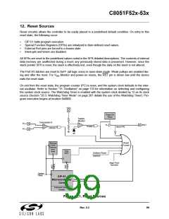
C8051F52x-53x
inverting input voltage (on CP0+) is less than the inverting input voltage (on CP0-), the device is put into
the reset state. After a Comparator0 reset, the C0RSEF flag (RSTSRC.5) will read ‘1’ signifying
Comparator0 as the reset source; otherwise, this bit reads ‘0’. The state of the RST pin is unaffected by
this reset.
12.6. PCA Watchdog Timer Reset
The programmable Watchdog Timer (WDT) function of the Programmable Counter Array (PCA) can be
used to prevent software from running out of control during a system malfunction. The PCA WDT function
can be enabled or disabled by software as described in Section “20.3. Watchdog Timer Mode” on
page 207; the WDT is enabled and clocked by SYSCLK / 12 following any reset. If a system malfunction
prevents user software from updating the WDT, a reset is generated and the WDTRSF bit (RSTSRC.5) is
set to ‘1’. The state of the RST pin is unaffected by this reset.
12.7. Flash Error Reset
If a Flash read/write/erase or program read targets an illegal address, a system reset is generated. This
may occur due to any of the following:
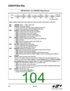
•
•
•
•
•
A Flash write or erase is attempted above user code space. This occurs when PSWE is set to ‘1’ and a
MOVX write operation targets an address above the Lock Byte address.
A Flash read is attempted above user code space. This occurs when a MOVC operation targets an
address above the Lock Byte address.
A Program read is attempted above user code space. This occurs when user code attempts to branch
to an address above the Lock Byte address.
A Flash read, write or erase attempt is restricted due to a Flash security setting (see Section
“13.4. Security Options” on page 112).
A Flash write or erase is attempted while the V Monitor is disabled.
DD
The FERROR bit (RSTSRC.6) is set following a Flash error reset. The state of the RST pin is unaffected by
this reset.
12.8. Software Reset
Software may force a reset by writing a ‘1’ to the SWRSF bit (RSTSRC.4). The SWRSF bit will read ‘1’ fol-
lowing a software forced reset. The state of the RST pin is unaffected by this reset.
Rev. 0.3
103

 SILICON [ SILICON ]