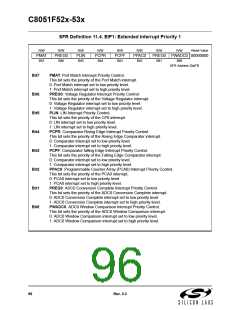
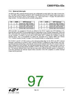
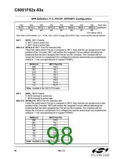
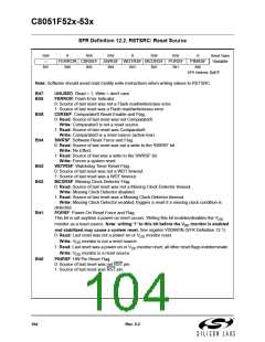
C8051F52x-53x
12.1. Power-On Reset
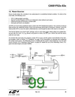
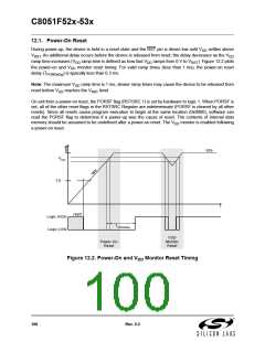
During power-up, the device is held in a reset state and the RST pin is driven low until V settles above
DD
V
. An additional delay occurs before the device is released from reset; the delay decreases as the V
DD
RST
ramp time increases (V ramp time is defined as how fast V ramps from 0 V to V ). Figure 12.2 plots
RST
DD
DD
the power-on and V
monitor reset timing. For valid ramp times (less than 1 ms), the power-on reset
DD
delay (T
) is typically less than 0.3 ms.
PORDelay
Note: The maximum V ramp time is 1 ms; slower ramp times may cause the device to be released from
DD
reset before V reaches the V
level.
RST
DD
On exit from a power-on reset, the PORSF flag (RSTSRC.1) is set by hardware to logic 1. When PORSF is
set, all of the other reset flags in the RSTSRC Register are indeterminate (PORSF is cleared by all other
resets). Since all resets cause program execution to begin at the same location (0x0000), software can
read the PORSF flag to determine if a power-up was the cause of reset. The contents of internal data
memory should be assumed to be undefined after a power-on reset. The V monitor is enabled following
DD
a power-on reset.
VDD
VRST
1.0
t
/RST
Logic HIGH
TPORDelay
Logic LOW
VDD
Power-On
Reset
Monitor
Reset
Figure 12.2. Power-On and V Monitor Reset Timing
DD
100
Rev. 0.3

 SILICON [ SILICON ]