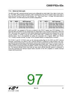
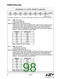
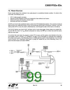
C8051F52x-53x
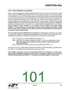
12.2. Power-Fail Reset / V Monitor
DD
When a power-down transition or power irregularity causes V
to drop below V , the power supply
RST
DD
monitor will drive the RST pin low and hold the CIP-51 in a reset state (see Figure 12.2). When V returns
DD
to a level above V , the CIP-51 will be released from the reset state. Note that even though internal data
RST
memory contents are not altered by the power-fail reset, it is impossible to determine if V dropped below
DD
the level required for data retention. If the PORSF flag reads ‘1’, the data may no longer be valid. The V
DD
monitor is enabled and is not selected as a reset source after power-on resets; however its defined state
(enabled/disabled) is not altered by any other reset source. For example, if the V monitor is disabled by
DD
software, and a software reset is performed, the V monitor will still be disabled after the reset. To pro-
DD
tect the integrity of Flash contents, the V
monitor must be enabled to the higher setting
DD
(VDMLVL = '1') and selected as a reset source if software contains routines which erase or write
Flash memory. If the V monitor is not enabled, any erase or write performed on Flash memory
DD
will cause a Flash Error device reset.
The V monitor must be enabled before it is selected as a reset source. Selecting the V monitor
DD
DD
as a reset source before it is enabled and stabilized may cause a system reset. The procedure for re-
enabling the V monitor and configuring the V monitor as a reset source is shown below:
DD
DD
Step 1. Enable the V monitor (VDMEN bit in VDM0CN = ‘1’).
DD
Step 2. Wait for the V monitor to stabilize (see Table 12.1 for the V Monitor turn-on time).
DD
DD
Note: This delay should be omitted if software contains routines which erase or
write Flash memory.
Step 3. Select the V monitor as a reset source (PORSF bit in RSTSRC = ‘1’).
DD
See Figure 12.2 for V monitor timing; note that the reset delay is not incurred after a V monitor reset.
DD
DD
See Table 12.1 for complete electrical characteristics of the V monitor.
DD
Note: Software should take care not to inadvertently disable the V
Monitor as a reset source
DD
when writing to RSTSRC to enable other reset sources or to trigger a software reset. All writes to
RSTSRC should explicitly set PORSF to '1' to keep the V Monitor enabled as a reset source.
DD
Rev. 0.3
101

 SILICON [ SILICON ]