C8051F52x-53x
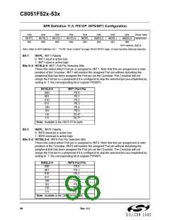
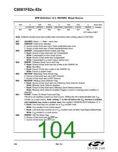
SFR Definition 12.1. VDDMON: V Monitor Control
DD
R/W
R
R/W
R
R
R
R
R
Reset Value
VDDMON VDDSTAT VDMLVL Reserved Reserved Reserved Reserved Reserved 1v000000
Bit7
Bit6
Bit5
Bit4
Bit3
Bit2
Bit1
Bit0
SFR Address:
0xFF
Bit7:
VDDMON: V Monitor Enable.
DD
This bit turns the V monitor circuit on/off. The V Monitor cannot generate system resets
DD
DD
until it is also selected as a reset source in register RSTSRC (SFR Definition 12.2). The V
DD
Monitor can be allowed to stabilize before it is selected as a reset source. Selecting the
V
monitor as a reset source before it has stabilized may generate a system reset.
DD
See Table 12.1 for the minimum V Monitor turn-on time.
DD
0: V Monitor Disabled.
DD
1: V Monitor Enabled (default).
DD
Bit6:
Bit5:
VDDSTAT: V Status.
DD
This bit indicates the current power supply status (V Monitor output).
DD
0: V is at or below the V Monitor Threshold.
DD
DD
1: V is above the V Monitor Threshold.
DD
DD
VDMLVL: V Level Select.
DD
0: V Monitor Threshold is set to V
(default).
DD
RST-LOW
RST-HIGH
1: V Monitor Threshold is set to V
. This setting is required for any system that
DD
includes code that writes to and/or erases Flash.
Bits4–0: RESERVED. Read = Variable. Write = don’t care.
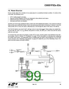
12.3. External Reset
The external RST pin provides a means for external circuitry to force the device into a reset state. Assert-
ing an active-low signal on the RST pin generates a reset; an external pullup and/or decoupling of the RST
pin may be necessary to avoid erroneous noise-induced resets. See Table 12.1 for complete RST pin
specifications. The PINRSF flag (RSTSRC.0) is set on exit from an external reset.
12.4. Missing Clock Detector Reset
The Missing Clock Detector (MCD) is a one-shot circuit that is triggered by the system clock. If the system
clock remains high or low for more than 100 µs, the one-shot will time out and generate a reset. After a
MCD reset, the MCDRSF flag (RSTSRC.2) will read ‘1’, signifying the MCD as the reset source; otherwise,
this bit reads ‘0’. Writing a ‘1’ to the MCDRSF bit enables the Missing Clock Detector; writing a ‘0’ disables
it. The state of the RST pin is unaffected by this reset.
12.5. Comparator Reset
Comparator0 can be configured as a reset source by writing a ‘1’ to the C0RSEF flag (RSTSRC.5).
Comparator0 should be enabled and allowed to settle prior to writing to C0RSEF to prevent any turn-on
chatter on the output from generating an unwanted reset. The Comparator0 reset is active-low: if the non-
102
Rev. 0.3

 SILICON [ SILICON ]