LOW CURRENT CONSUMPTION HIGH RIPPLE-REJECTION LOW DROPOUT CMOS VOLTAGE REGULATOR
Rev.2.3_01
S-1312 Series
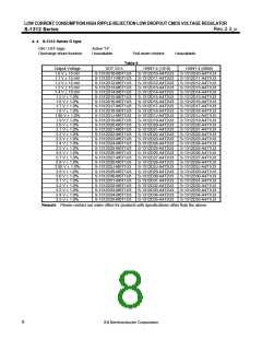
Electrical Characteristics
Table 12
(Ta = +25°C unless otherwise specified)
Test
Circuit
Item
Symbol
Condition
Min.
Typ.
Max.
Unit
VOUT(S)
VOUT(S)
1.0 V
1.5 V
≤
≤
VOUT(S) < 1.5 V
VOUT(S) 3.5 V
VOUT(S)
VOUT(S)
V
1
−
0.015
+
0.015
V
IN = VOUT(S)
+
+
1.0 V,
1.0 V
Output voltage*1
VOUT(E)
I
OUT = 30 mA
VOUT(S)
VOUT(S)
≤
V
1
×
0.99
×
1.01
Output current*2
IOUT
VIN
≥
VOUT(S)
150*5
−
−
mA
V
3
1
1
1
1
1
1
1
1
1
1
1
1.0 V
1.1 V
1.2 V
1.3 V
1.4 V
1.5 V
1.7 V
2.0 V
2.5 V
3.0 V
3.3 V
≤
≤
≤
≤
≤
≤
≤
≤
≤
≤
≤
VOUT(S) < 1.1 V
VOUT(S) < 1.2 V
VOUT(S) < 1.3 V
VOUT(S) < 1.4 V
VOUT(S) < 1.5 V
VOUT(S) < 1.7 V
VOUT(S) < 2.0 V
VOUT(S) < 2.5 V
VOUT(S) < 3.0 V
VOUT(S) < 3.3 V
0.50
−
−
−
−
−
−
−
−
0.68
0.52
0.31
0.28
0.26
0.24
0.22
0.18
0.16
0.15
0.14
0.86
0.71
0.63
0.56
0.50
0.47
0.43
0.36
0.32
0.28
0.27
V
V
V
V
Dropout voltage*3
Vdrop
IOUT = 100 mA
V
V
V
V
−
−
V
VOUT(S)
≤
3.5 V
V
1.0 V
1.6 V
1.1 V
≤
≤
≤
VOUT(S) < 1.1 V
VIN 5.5V, IOUT = 30 mA
VOUT(S)
0.5 V
−
0.02
0.1
%/V
1
Δ
VOUT1
≤
Line regulation
Load regulation
≤
≤
3.5 V
VIN
Δ
VIN
• VOUT
−
−
0.02
20
0.1
40
%/V
mV
1
1
VOUT(S)
VIN = VOUT(S)
IN = VOUT(S)
40
+
≤
5.5 V, IOUT = 30 mA
ΔVOUT2
+
1.0 V, 100
μA
≤
IOUT
≤ 100 mA
Δ
VOUT
Output voltage
temperature coefficient*4
V
+
1.0 V, IOUT
=
30 mA,
−
−
130
20
−
ppm/
°
C
1
2
−
°
C
≤
Ta ≤ + 85
°
C
Δ
Ta
•
VOUT
Current consumption
during operation
Current consumption
during power-off
Input voltage
ISS1
VIN = VOUT(S)
VIN = VOUT(S)
+
+
1.0 V, ON / OFF pin = ON, no load
30
μA
ISS2
VIN
1.0 V, ON / OFF pin = OFF, no load
−
0.1
−
1.0
5.5
−
μA
2
−
4
−
1.5
1.0
V
V
IN = VOUT(S)
+
1.0 V, RL = 1.0 kΩ
ON / OFF pin input voltage "H" VSH
−
V
V
determined by VOUT output level
V
IN = VOUT(S) + 1.0 V, RL = 1.0 kΩ
ON / OFF pin input voltage "L"
ON / OFF pin input current "H"
ON / OFF pin input current "L"
VSL
ISH
ISL
−
−
−
0.25
0.1
4
4
4
4
determined by VOUT output level
B / D type
(without pull-down registor)
A / C type
−
0.1
μ
A
A
A
V
V
IN = 5.5 V,
ON / OFF = 5.5 V
1.0
2.5
−
5.0
μ
μ
(with pull-down registor)
VIN = 5.5 V, VON / OFF = 0 V
−
0.1
0.1
1.0 V
≤
VOUT(S)
≤
≤
1.2 V
−
−
75
70
−
−
dB
dB
5
5
V
IN = VOUT(S)
f = 1.0 kHz,
Vrip = 0.5 Vrms,
IOUT = 30 mA
+ 1.0 V,
RR
Ripple rejection
1.2 V < VOUT(S)
2.85 V
Δ
2.85 V < VOUT(S)
≤
3.5 V
−
−
65
50
−
−
dB
5
3
Short-circuit current
Thermal shutdown detection
temperature
Ishort
TSD
VIN = VOUT(S)
+
1.0 V, ON / OFF pin = ON, VOUT = 0 V
mA
Junction temperature
Junction temperature
−
−
150
120
35
−
−
°
°
C
C
−
−
3
4
Thermal shutdown
release temperature
TSR
V
V
OUT = 0.1 V,
IN = 5.5 V
A / B type
"L" output Nch ON resistance
RLOW
−
−
Ω
(with discharge shuntfunction)
A / C type
Power-off pull-down resistance RPD
−
1.0
2.2
5.0
MΩ
(with pull-down registor)
12

 SII [ SEIKO INSTRUMENTS INC ]