LOW CURRENT CONSUMPTION HIGH RIPPLE-REJECTION LOW DROPOUT CMOS VOLTAGE REGULATOR
Rev.2.3_01
S-1312 Series
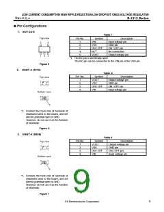
Pin Configurations
1. SOT-23-5
Table 7
Top view
Pin No.
Symbol
VIN
Description
Input voltage pin
1
2
3
4
5
5
4
VSS
GND pin
ON / OFF
NC*1
ON / OFF pin
No connection
VOUT
Output voltage pin
1
2
3
*1. The NC pin is electrically open.
The NC pin can be connected to the VIN pin or the VSS pin.
Figure 5
2. HSNT-4 (1010)
Table 8
Pin No.
Symbol
VOUT
Description
Output voltage pin
Top view
1
2
3
4
1
2
4
3
VSS
GND pin
ON / OFF
VIN
ON / OFF pin
Input voltage pin
Bottom view
4
3
1
2
*1
*1. Connect the heat sink of backside at
shadowed area to the board, and set
electric potential open or GND.
However, do not use it as the function
of electrode.
Figure 6
3. HSNT-4 (0808)
Table 9
Pin No.
Symbol
VOUT
Description
Top view
1
2
3
4
Output voltage pin
GND pin
1
2
4
3
VSS
ON / OFF
VIN
ON / OFF pin
Input voltage pin
Bottom view
4
3
1
2
*1
*1. Connect the heat sink of backside at
shadowed area to the board, and set
electric potential open or GND.
However, do not use it as the function
of electrode.
Figure 7
9

 SII [ SEIKO INSTRUMENTS INC ]