LOW CURRENT CONSUMPTION HIGH RIPPLE-REJECTION LOW DROPOUT CMOS VOLTAGE REGULATOR
Rev.2.3_01
S-1312 Series
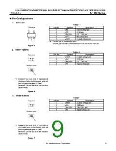
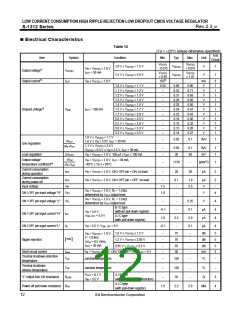
*1. VOUT(S): Set output voltage
VOUT(E): Actual output voltage
Output voltage when fixing IOUT (= 30 mA) and inputting VOUT(S) + 1.0 V
*2. The output current at which the output voltage becomes 95% of VOUT(E) after gradually increasing the output current.
*3. Vdrop = VIN1 − (VOUT3 × 0.98)
VOUT3 is the output voltage when VIN = VOUT(S) + 1.0 V and IOUT = 100 mA.
VIN1 is the input voltage at which the output voltage becomes 98% of VOUT3 after gradually decreasing the input
voltage.
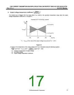
*4. A change in the temperature of the output voltage [mV/°C] is calculated using the following equation.
ΔVOUT
ΔTa
ΔVOUT
ΔTa•VOUT
mV/°C *1 = VOUT(S) V *2
×
ppm/°C *3 ÷ 1000
[ ]
[
]
[ ]
*1. Change in temperature of output voltage
*2. Set output voltage
*3. Output voltage temperature coefficient
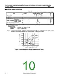
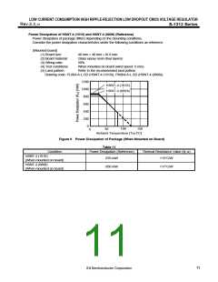
*5. The output current can be at least this value.
Due to restrictions on the package power dissipation, this value may not be satisfied. Attention should be paid to the
power dissipation of the package when the output current is large.
This specification is guaranteed by design.
13

 SII [ SEIKO INSTRUMENTS INC ]