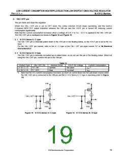
LOW CURRENT CONSUMPTION HIGH RIPPLE-REJECTION LOW DROPOUT CMOS VOLTAGE REGULATOR
Rev.2.3_01
S-1312 Series
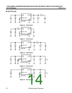
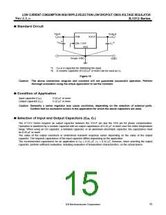
Standard Circuit
Input
CIN
Output
VIN
VOUT
*1
*2
ON / OFF
CL
VSS
Single GND
GND
*1.
CIN is a capacitor for stabilizing the input.
*2. A ceramic capacitor of 0.22 μF or more can be used as CL.
Figure 15
Caution The above connection diagram and constant will not guarantee successful operation. Perform
thorough evaluation using the actual application to set the constant.
Condition of Application
Input capacitor (CIN):
Output capacitor (CL):
0.22 μF or more
0.22 μF or more
Caution Generally a series regulator may cause oscillation, depending on the selection of external parts.
Confirm that no oscillation occurs in the application for which the above capacitors are used.
Selection of Input and Output Capacitors (CIN, CL)
The S-1312 Series requires an output capacitor between the VOUT pin and the VSS pin for phase compensation.
Operation is stabilized by a ceramic capacitor with an output capacitance of 0.22 μF or more over the entire temperature
range. When using an OS capacitor, a tantalum capacitor, or an aluminum electrolytic capacitor, the capacitance must
be 0.22 μF or more.
The value of the output overshoot or undershoot transient response varies depending on the value of the output
capacitor. The required capacitance of the input capacitor differs depending on the application.
The recommended capacitance for an application is CIN ≥ 0.22 μF, CL ≥ 0.22 μF; however, when selecting the output
capacitor, perform sufficient evaluation, including evaluation of temperature characteristics, on the actual device.
15

 SII [ SEIKO INSTRUMENTS INC ]