LC89057W-VF4A-E
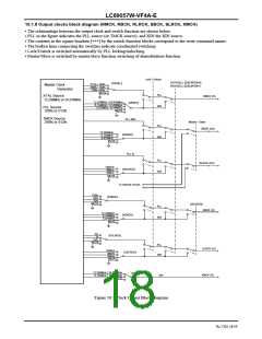
10.1.7 Output clocks (RMCK, RBCK, RLRCK, SBCK, SLRCK)
•
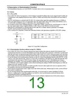
The LC89057W-VF4A-E features two clock systems (R and S systems) in order to supply the various needed clocks
to peripheral devices such as A/D converter and DSP.
•
The clock output settings for the R and S systems are done with PRSEL[1:0], XRSEL[1:0], XRBCK[1:0],
XRLRCK[1:0], PSBCK[1:0], PSLRCK[1:0], XSBCK[1:0], and XSLRCK[1:0].
•
Setting range for each clock output pin when the PLL is used as source
(1) RMCK: Selection from 1/1, 1/2, and 1/4 of 512fs or 256fs
(2) RBCK: 64fs output
(3) RLRCK: fs output
(4) SBCK: Selection from 128fs, 64fs, and 32fs
(5)SLRCK: Selection from 2fs, fs, and fs/2
•
Setting range for each clock output pins when the XIN is used as source
(1) RMCK: Selection from 1/1, 1/2, and 1/4 of 12.288MHz or 24.576MHz
(2) RBCK: Selection from 12.288MHz, 6.144MHz, and 3.072MHz
(3) SBCK: Selection from 12.288MHz, 6.144MHz, and 3.072MHz
(4) RLRCK: Selection from 192kHz, 96kHz, and 48kHz
(5) SLRCK: Selection from 192kHz, 96kHz, and 48kHz
•
Setting range for each clock output pins when the TMCK is used as source
(1) RMCK: selection from 1/1, 1/2,1/4 of 512fs or 256fs.
(2) RBCK: 64fs output
(3) RLRCK: fs output
(4) SBCK: selection from 128fs, 64fs, 32fs
(5) SLRCK: selection from 2fs, fs, fs/2
•
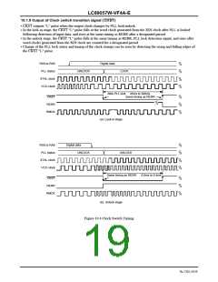
The polarity of RBCK, RLRCK, SBCK, and SLRCK can be reversed with RBCKP, RLRCKP, SBCKP, and SLRCKP.
•
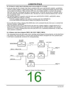
Clock switching is processed from the rising edge of RLRCK output after the falling edge of microcontroller interface
CE.
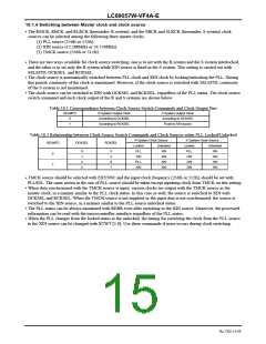
Table 10.3 List of Output Clock Frequencies (Bold Items = Initial Settings)
PLL Source (Internal VCO CK)
TMCK Source (TMCK input CK)
XIN Source (XIN input CK)
Output Pin Name
RMCK
512fs
256fs
512fs
256fs
12.288MHz
24.576MHz
512fs
256fs
128fs
256fs
128fs
64fs
512fs
256fs
128fs
256fs
128fs
64fs
12.288MHz
6.144MHz
3.072MHz
24.576MHz
12.288MHz
6.144MHz
12.288MHz
RBCK
RLRCK
SBCK
64fs
fs
6.144MHz
3.072MHz
192kHz
96kHz
48kHz
128fs
64fs
32fs
12.288MHz
6.144MHz
3.072MHz
2fs
fs
192kHz
96kHz
48kHz
SLRCK
fs/2
No.7202-17/59

 SANYO [ SANYO SEMICON DEVICE ]