LC89057W-VF4A-E
____________
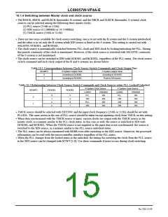
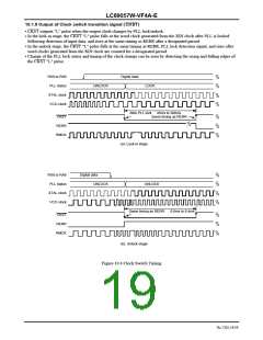
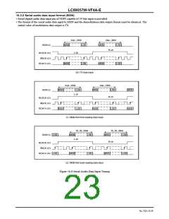
10.1.9 Output of Clock switch transition signal (CKST)
__________
•
•
CKST outputs "L" pulse when the output clock changes by PLL lock/unlock.
In the lock-in stage, the CKST "L" pulse falls at the word clock generated from the XIN clock after PLL is locked
__________
following detection of input data, and rises at the same timing as RERR after a designated period.
__________
•
•
In the unlock stage, the CKST "L" pulse falls at the same timing as RERR, PLL lock detection signal, and rises after
word clocks generated from the XIN clock are counted for a designated period.
Change of the PLL lock status and timing of the clock change can be seen by detecting the rising and falling edges of
__________
the CKST "L" pulse.
RX0 to RX6
PLL status
XTAL clock
VCO clock
Digital data
UNLOCK
LOCK
After PLL lock 45ms to 300ms
Same timing as RERR
CKST
RERR
RMCK
(a): Lock-in stage
RX0 to RX6
PLL status
XTAL clock
VCO clock
Digital data
UNLOCK
UNLOCK
Same timing as RERR
0.6ms to 6.4ms
CKST
RERR
RMCK
(b): Unlock stage
Figure 10.4 Clock Switch Timing
No.7202-19/59

 SANYO [ SANYO SEMICON DEVICE ]