LC89057W-VF4A-E
10.2 Bi-phase Signal I/O
10.2.1 Reception range of bi-phase signal input
•
Reception range of the input data depends on the PLL lock frequency setting done with PLLSEL. The relationship
between this setting and the guaranteed reception range is shown below.
Table 10.4 Relationship between PLL Output Clock Setting and Reception Range (FSLIM [1:0] = 00)
PLL Output Clock Setting
512fs (PLLSEL = 0)
256fs (PLLSEL = 1)
Input Data Reception Range
28kHz to 105kHz
28kHz to 195kHz
•
The fs reception range for input data can be limited within the set range of PLL output clocks stated above. This
setting is carried out with FSLIM [1:0]. When this function is adopted, input data exceeding the set range is
considered as an error, the clock source is automatically switched to the XIN source, and RDATA output data is
subject to the RDTSEL setting.
10.2.2 Bi-phase signal I/O pins (RX0 to RX6, RXOUT)
•
There are 7 kinds of digital data input pins. Moreover, data modulated with the modulation function is also available
and thus there are 8 options in total. However, the pins to be selected are restricted, depending on the setting
conditions.
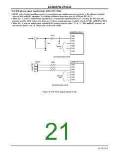
(1) The six pins of RX0 and RX2 to RX6 are TTL level input pins with 5V-tolerance voltage.
(2) RX1 is an input pin with built-in amplifier, which is coaxial-compatible and it, can receive up to min,
200mVp-p data.
•
The demodulation input and RXOUT output signals could each be selected independently.
(1) The demodulation data is selected with RISEL [2:0].
(2) The RXOUT output data is selected with ROSEL [2:0].
•
RXOUT can be muted with RXOFF. Muting is recommended to reduce clock jitter when RXOUT is not used.
•
The data input status can be monitored with the RXMON setting. The status of each data input pin is stored in CCB
address 0xEA and output registers DO0 to DO7. Since this function uses the XIN clock, the oscillation amplifier must
be set to the continuous operation mode when RXMON is set.
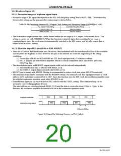
•
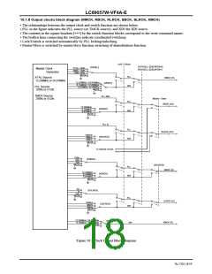
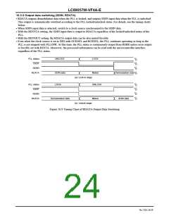
Demodulation input pin can be switched via PLL unlock with the ULSEL setting. Thus data switching can be
accurately conveyed to peripheral devices.
The interval from pin switching through RISEL [2:0] until the data is received is about 250μs to 350μs. In this
function, the oscillation amplifier also needs to be set to the continuous operation mode.
RX0
RX2
RX3
RX1
Input pin selection
RX0
RX2
RX3
RX1
Internal supply signal
250μs to 350μs
Figure 10.5 Input Pin Selecting Process via PLL Unlock
No.7202-20/59

 SANYO [ SANYO SEMICON DEVICE ]