LC89057W-VF4A-E
10.1.5 Points to notice about switching clock source while PLL is locked
•
In the state where the PLL is locked, if the clock is switched to XIN source with SELMTD, OCKSEL, and RCKSEL
while the oscillator amplifier is stopped (initial setting), clock continuity is maintained but RERR temporarily outputs
an error (high level) indication. When switched to XIN source, the oscillator amplifier is switched to the operating
state at the same time. Consequently the input fs calculation restarts. At this time, the previous fs calculation value is
reset and compared with the newly calculated fs value. Then those two values are found not identical, that’s why the
error is temporarily issued.
•
The following settings are required to switch the clock source with SELMTD, OCKSEL, and RCKSEL without
changing the RERR status while PLL is locked.
(1) Set the oscillation amplifier to the continuous operation mode with AMPOPR[1:0].
(2) Set with FSERR to the mode where fs change is not reflected to the error flag.
•
By one of the above settings, changing of the RERR status can be constrained when the clock source is switched with
SELMTD, OCKSEL, and RCKSEL.
•
When switching the clock source to XIN from the state where the oscillation amplifier is stopped while the PLL is
locked, the output clock using XIN as the source starts being output after the oscillation amplifier starts operating.
When the PLL is locked, switching of the clock source from XIN to PLL is performed instantaneously. In either case,
clock continuity is maintained.
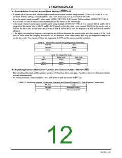
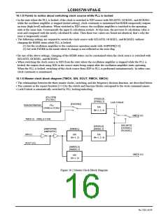
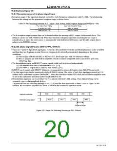
10.1.6 Master clock block diagram (TMCK, XIN, XOUT, RMCK, XMCK)
•
The relationships between the three master clocks, switching, and the frequency division function, are described below.
•
The contents in the square brackets [∗∗∗] by the switch and function blocks correspond to the write command names.
Lock/Unlock is automatically switched by PLL locking/unlocking.
•
[PLLOPR]
[PRSEL0]
[PLLSEL]
[PRSEL1]
Lock /Unlock
[EXSYNC]
Selected Biphase
PLL
1/N
(256fs or 512fs)
(N=1, 2, 4)
RMCK (O)
TMCK (I) 256fs or 512fs
[SELMTD]
[OCKSEL]
[RCKSEL]
[XRSEL0]
[XRSEL1]
[AMPOPR0]
[AMPOPR1]
[XINSEL]
XIN (I)
1/N
1/N
(N=1, 2)
(N=1, 2, 4)
XOUT (O)
[XMSEL0]
[XMSEL1]
XMCK (O)
1/N
(N=1, 2)
Figure 10.2 Master Clock Block Diagram
No.7202-16/59

 SANYO [ SANYO SEMICON DEVICE ]