LC72722, 72722M, 72722PM
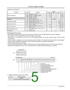
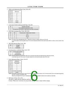
2. Offset word information flag (3 bits): B0 to B2
B
2
B
1
B
0
Offset word
0
0
0
0
1
1
1
1
0
0
1
1
0
0
1
1
0
1
0
1
0
1
0
1
A
B
C
C’
D
E
Unused
Unused
3. Consecutive RAM readout possible flag (1 bit): RE
RE
1
RAM data information
The next data to be read out is in RAM.
0
This data item is the last item in RAM, and the next data is not present.
4. RAM data remaining flag (2 bits): RF0, RF1
RF1
0
RF0
0
Remaining data in RAM (number of blocks)
1 to 7
8 to 15
16 to 23
24
0
1
1
0
1
1
Caution: This value is only meaningful when RE is 1. When RE is 0, there is no data in RAM, even if RF is 00.
If a synchronization reset was applied using SYR, then the backward protection block data that was written to memory is also counted in this
value.
5. ARI (SK) detection flag (1 bit): ARI
ARI
1
SK signal
Detected
0
Not detected
6. Synchronization established flag (1 bit): SYC
SYC
Synchronization detection
Synchronized
1
0
Not synchronized
Caution: This flag indicates the synchronization state of the circuit at the point where the data block being output was received.
On the other hand, the SYNC pin (pin 18) output indicates the current synchronization state of the circuit.
7. Error information flags (3 bits): E0 to E2
E
2
E
1
E
0
Number of
bits corrected
0
0
0
0
1
1
1
1
0
0
1
1
0
0
1
1
0
1
0
1
0
1
0
1
0 (no errors)
1
2
3
4
5
Correction not possible
Unused
Caution: If the number of errors exceeds the value of the EC0 to EC2 setting (see the section on the CCB input format), the error information flags will be
set to the “Correction not possible” value.
When the error flags E0 to E2 are 011 (indicating that correction is not possible) the data must be handled as invalid data.
8. RDS data (16 bits): D0 to D15
This data is output with the MSB first and the LSB last.
Caution: When error correction was not possible, the input data is output without change.
No. 5602-6/15

 SANYO [ SANYO SEMICON DEVICE ]