LC72722, 72722M, 72722PM
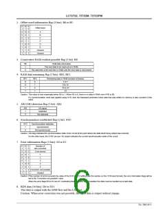
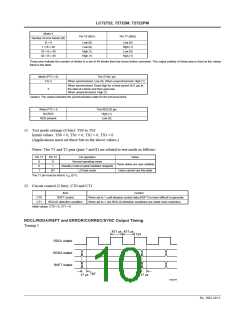
Mode 4
Number of error blocks (B)
B = 0
Pin T6 (BE1)
Pin T7 (BE0)
Low (0)
Low (0)
High (1)
High (1)
Low (0)
High (1)
Low (0)
High (1)
1 ≤ B ≤ 20
20 < B ≤ 40
40 < B ≤ 48
These pins indicate the number of blocks in a set of 48 blocks that had errors before correction. The output polarity of these pins is fixed at the values
listed in the table.
Mode (PT2 = 0)
0 to 2
The SYNC pin
When synchronized: Low (0). When unsynchronized: High (1)
When synchronized: Goes high for a fixed period (421 µs) at
the start of a block and then goes low.
3
When unsynchronized: High (1)
Caution: The output indicates the synchronization state for the previous block.
When PT2 = 0
No RDS
The RDS-ID pin
High (1)
RDS present
Low (0)
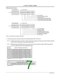
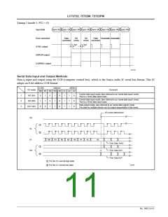
11. Test mode settings (4 bits): TS0 to TS3
Initial values: TS0 = 0, TS1 = 0, TS2 = 0, TS3 = 0
(Applications must set these bits to the above values.)
Notes: The T1 and T2 pins (pins 7 and 8) are related to test mode as follows:
Pin T1
Pin T2
LSI operation
Normal operating mode
Notes
0
0
1
0
1
These states are user settable
Users cannot use this state
Standby mode (crystal oscillator stopped)
LSI test mode
0/1
The T1 pin must be tied to VSS (0 V).
12. Circuit control (2 bits): CT0 and CT1
Item
Control
CT0
CT1
RSFT control
When set to 1, soft-decision control data (RSFT) is more difficult to generate.
When set to 1, the RDS-ID detection conditions are made more restrictive.
RDS-ID detection condition
Initial values: CT0 = 0, CT1 = 0
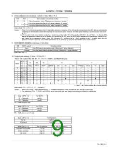
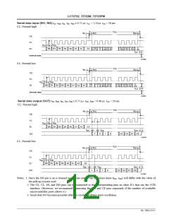
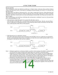
RDCL/RDDA/RSFT and ERROR/CORREC/SYNC Output Timing
Timing 1
421 µs 421 µs
Tp1
RDCL output
RDDA output
RSFT output
Tp2
17 µs
17 µs
A12377
No. 5602-10/15

 SANYO [ SANYO SEMICON DEVICE ]