LC72722, 72722M, 72722PM
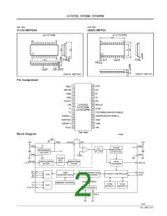
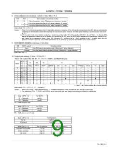
Pin Functions
Pin No.
Pin name
Function
I/O
Pin circuit
Vdda
1
VREF
Reference voltage output (Vdda/2)
Output
Vssa
Vdda
A12365
2
MPXIN
Baseband (multiplexed) signal input
Input
Vssa
A12366
–
+
5
6
FLOUT
Subcarrier output (filter output)
Output
Input
A12367
Vdda
CIN
Subcarrier input (comparator input)
Vssa
A12368
V
REF
3
4
Vdda
Vssa
Analog system power supply (+5 V)
Analog system ground
—
—
—
—
Vddd
12
13
XOUT
XIN
Crystal oscillator output (4.332/8.664 MHz)
Output
X
IN
X
Vssd
OUT
Crystal oscillator input (external reference signal input)
Test input (This pin must always be connected to ground.)
A12369
A12370
7
8
T1
T2
Input
S
Test input (standby control)
0: Normal operation, 1: Standby state (crystal oscillator stopped)
Vssd
9
T3 (RDCL)
T4 (RDDA)
T5 (RSFT)
Test I/O (RDS clock output)
10
11
Test I/O (RDS data output)
Test I/O (soft-decision control data output)
Test I/O (error status output, regenerated carrier output,
TP output, error block count output)
16
T6 (ERROR/57K/TP/BE1)
I/O*
Vssd
A12371
Test I/O (Error correction status output, SK detection output,
TA output, error block count output)
17 T7 (CORREC/ARI-ID/TA/BE0)
18
19
SYNC
Block synchronization detection output
RDS detection output
RDS-ID
Output
Input
Vssd
20
DO
Data output
A12372
A12373
21
22
23
24
14
15
CL
DI
Clock input
Serial data interface (CCB)
S
Data input
CE
Chip enable
Vssd
SYR
Vddd
Vssd
Synchronization and RAM address reset (active high)
Digital system power supply (+5 V)
Digital system ground
—
—
—
—
Note: * Normally function as an output pin. Used as an I/O pin in test mode, which is not available to user applications.
No. 5602-3/15

 SANYO [ SANYO SEMICON DEVICE ]