LC72722, 72722M, 72722PM
Continued from preceding page.
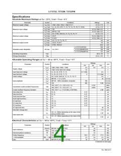
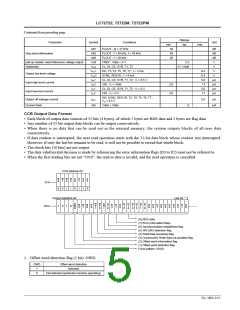
Ratings
typ
Parameter
Symbol
Conditions
FLOUT : ∆f = ±7 kHz
Unit
min
30
max
Att1
Att2
Att3
Vref
VHIS
dB
dB
dB
V
Stop band attenuation
FLOUT : f < 45 kHz, f > 70 kHz
FLOUT : f < 20 kHz
40
50
pull-up resistor used.Reference voltage output
Hysteresis
VREF : Vdda = 5 V
2.5
CL, DI, CE, SYR, T1, T2
DO, T3, T4, T5, T6, T7 : I = 2 mA
SYNC, RDS-ID : I = 8 mA
CL, DI, CE, SYR, T1, T2 : VI = 6.5 V
XIN : VI = Vddd
0.1 Vddd
V
V
OL1
OL2
0.4
V
Output low-level voltage
Input high-level current
Input low-level current
V
0.4
5.0
11
V
IIH1
µA
µA
µA
µA
IIH2
2.0
2.0
IIL1
IIL2
CL, DI, CE, SYR, T1, T2 : VI = 0 V
XIN : VI = 0 V
5.0
11
DO, SYNC, RDS-ID, T3, T4, T5, T6, T7 :
Output off leakage current
Current drain
IOFF
Idd
5.0
µA
VO = 6.5 V
Vddd + Vdda
9
mA
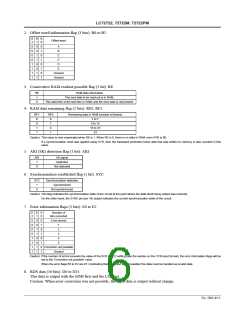
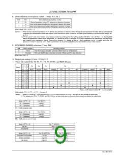
CCB Output Data Format
• Each block of output data consists of 32 bits (4 bytes), of which 2 bytes are RDS data and 2 bytes are flag data.
• Any number of 32-bit output data blocks can be output consecutively.
• When there is no data that can be read out in the internal memory, the system outputs blocks of all-zero data
consecutively.
• If data readout is interrupted, the next read operation starts with the 32-bit data block whose readout was interrupted.
However, if only the last bit remains to be read, it will not be possible to reread that whole block.
• The check bits (10 bits) are not output.
• The data valid/invalid decision is made by referencing the error information flags (E0 to E2) must not be referred to.
• When the first leading bits are not "1010", the read in data is invalid, and the read operation is cancelled.
CCB address 6C
B
0
B
1
B
2
B
3
A
0
A
1
A
2
A
3
DI
0
0
1
1
0
1
1
0
Output data/first bit
Last bit
O
R
F
1
R
F
0
A
R
I
S
Y
C
D
1
5
D
1
4
D
1
3
D
1
2
D
1
1
D
1
0
B
2
B
1
B
0
R
E
E
2
E
1
E
0
D D D D D D D D D D
1
0
1
0
DO
W
9
8
7
6
5
4
3
2
1
0
D
(8) RDS data
(7) Error information flags
(6) Synchronization established flag
(5) ARI (SK) detection flag
(4) RAM data remaining flag
(3) Consecutive RAM read out possible flag
(2) Offset word information flag
(1) Offset word detection flag
Fixed pattern (1010)
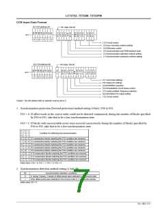
1. Offset word detection flag (1 bit): OWD
OWD
Offset word detection
Detected
1
0
Not detected (protection function operating)
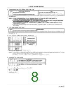
No. 5602-5/15

 SANYO [ SANYO SEMICON DEVICE ]