LC72722, 72722M, 72722PM
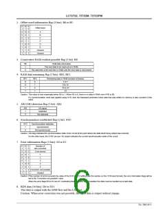
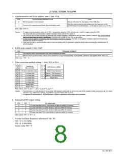
3. Synchronization and RAM address reset (1 bit): SYR
SYR
0
Synchronization detection circuit
Normal operation (reset cleared)
RAM
Normal write (See the description of the OWE bit.)
After the reset is cleared, start writing from the data prior to the
establishment of synchronization, i.e. the data in backward protection.
1
Forced to the unsynchronized state (synchronization reset)
Initial value: SYR =0
Caution: 1. To apply a synchronization reset, set SYR to 1 temporarily using the CCB, and then set it back to 0 again using the CCB.
The circuit will start synchronization capture operation at the point SYR is set to 0.
2. The SYR pin (pin 24) also provides an identical reset control operation. Applications can use either method. However, the control method
that is not used must be set to 0 at all times. Any pulse with a width of over 250 ns will suffice.
3. A reset must be applied immediately after the reception channel is changed. If a reset is not applied, reception data from the previous
channel may remain in memory.
4. Data read out after a synchronization reset is read out starting with the backward protection block data preceding the establishment of
synchronization.
4. RAM write control (1 bit): OWE
OWE
RAM write conditions
Only data for which synchronization had been established is written.
Data for which synchronization not has been established (unsynchronized data) is also written. (However, this applies when SYR = 0.)
0
1
Initial value: OWE = 0
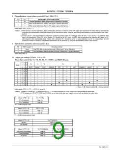
5. Error correction method setting (5 bits): EC0 to EC4
E
C
0
E
C
1
E
C
2
E
C
3
E
C
4
Number of
bits corrected
Soft-decision setting
0
1
0
1
0
1
0
1
0
0
1
1
0
0
1
1
0
0
0
0
1
1
1
1
0 (error detection only)
1 or fewer bits
2 or fewer bits
3 or fewer bits
4 or fewer bits
5 or fewer bits
Illegal value
0
1
0
1
0
0
1
1
Mode 0: Hard decision
Mode 1: Soft decision A
Mode 2: Soft decision B
Illegal value
Illegal value
Initial values: EC0 = 0, EC1 = 1, EC2 = 0, EC3 = 0, EC4 = 1
Caution: 1. If soft-decision A or soft-decision B is specified, soft-decision control will be performed even if the number of bits corrected is set to 0 (error
detection only). With these settings, data will be output for blocks with no errors.
2. As opposed to soft-decision B, the soft-decision A setting suppresses soft decision error correction.
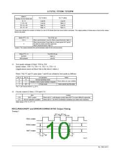
6. Intermittent DO output setting
SP0
0
SP1
0
DO output state
DO goes low when one or more blocks of data are written to memory.
DO goes low when 4 or more blocks of data are written to memory.
DO goes low when 8 or more blocks of data are written to memory.
DO goes low when 12 or more blocks of data are written to memory.
1
0
0
1
1
1
Initial values: SP0 = 0, SP1 = 0
7. Crystal oscillator frequency selection (1 bit): XS
XS = 0: 4.332 MHz
XS = 1: 8.664 MHz
Initial value: XS = 0
No. 5602-8/15

 SANYO [ SANYO SEMICON DEVICE ]