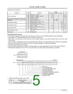
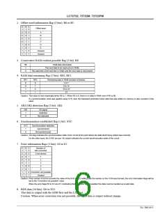
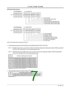
LC72722, 72722M, 72722PM
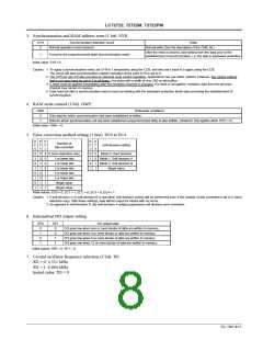
8. Demodulation circuit phase control (2 bits): PL0, PL1
PL0
0
PL1
0/1
0
Demodulation circuit phase control
<Normal operation> when ARI presence or absence is unclear.
If the circuit determines that the ARI signal is absent: 90° phase
If the circuit determines that the ARI signal is present: 0° phase
1
1
Initial values: PL0 = 0, PL1 = 1
Caution: 1. When PL0 is 0 (normal operation), the IC detects the presence or absence of the ARI signal and reproduces the RDS data by automatically
controlling the demodulation phase with respect to the reproduced carrier. However, the initial phase following a synchronization reset is set
by PL1.
2. If PL0 is set to 1, the demodulation circuit phase is locked according to the PL1 setting at either 90° (PL1 = 0) or 0° (PL1 = 1), allowing RDS
data to be reproduced. When ARI is not present, PL1 should be set to 0, since the RDS data is reproduced by detecting at a phase of 90°
with respect to the reproduced carrier. When ARI is present, PL1 should be set to 1, since detection is at 0°. In cases where the ARI
presence is known in advance, more stable reproduction can be achieved by fixing the demodulation phase in this manner.
9. RDS/RBDS (MMBS) selection (1 bit): RM
RM
0
RBDS support
None
Decoding method
Only RDS data is decoded correctly (Offset word E is not detected.)
RDS and MMBS data is decoded correctly (Offset word E is also detected.)
1
Provided
Initial value: RM = 0
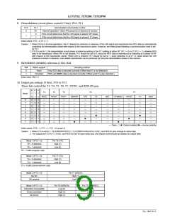
10. Output pin settings (3 bits): PT0 to PT2
These bits control the T3, T4, T5, T6, T7, SYNC, and RDS-ID pins.
P
T
0
0
1
0
1
0
1
0
1
P
T
1
0
0
1
1
0
0
1
1
P
T
2
0
0
0
0
1
1
1
1
T3
T4
T5
T6
T7
Mode
RDCL
—
RDDA
—
RSFT
—
ERROR
57K
—
—
●
TP
—
●
BE1
—
—
—
—
●
CORREC
ARI-ID
—
TA
—
●
BE0
—
—
—
—
●
0
1
2
3
4
5
6
7
—
—
—
●
—
—
—
●
—
—
—
—
●
●
●
—
—
—
●
●
—
—
—
●
●
●
●
—
—
—
●
—
—
—
—
—
—
—
●
—
—
—
●
—
—
—
—
—
—
—
—
—
—
—
●
●
●
—
—
●
—
—
●
●
●
—
—
—: Open, ●, ●: Output enabled (● = reverse polarity)
Initial values: PT0 = 1, PT1 = 1, PT2 = 0 (mode 3)
Caution: 1. When PT2 is set to 1, T6 (ERROR/57K/TP), T7 (CORREC/ARI-ID/TA) SYNC, and RDS-ID pins change to active high.
2. The output pins (T3 to T7, SYNC, and RDS-ID) are all open-drain pins, and require external pull-up resistors to output data.
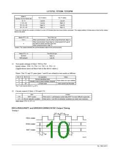
Mode 1 (PT2 = 0)
TP = 0 detected
Pin T6 (TP)
High (1)
TP = 1 detected
Low (0)
TP = Traffic program code
Mode 1 (PT2 = 0)
TA = 0 detected
Pin T7 (TA)
High (1)
TA = 1 detected
Low (0)
TA = Traffic announcement code
Mode 2 (PT2 = 0)
No SK
Pin T7 (ARI-ID)
High (1)
SK present
Low (0)
Mode 3 (PT2 = 0)
Correction not possible
Errors corrected
No errors
Pin T6 (ERROR)
Low (0)
Pin T7 (CORREC)
Low (0)
High (1)
Low (0)
High (1)
High (1)
No. 5602-9/15

 SANYO [ SANYO SEMICON DEVICE ]