S3C4510B
HDLC CONTROLLERS
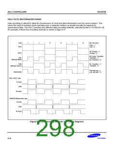
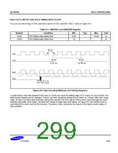
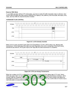
HDLC DATA SETUP AND HOLD TIMING WITH CLOCK
You can see the timing of TxD and RxD in terms of TxC and RxC HDLC clock in Figure 8-6.
Table 8-3. HMODEA and HMODEB Register
Symbol
Ttxdf
Condition
TxD falling edge delay time
TxD falling edge delay time
Min
9.82
1.0
Typ
Max
Unit
ns
10.66
Trxdf
ns
40 ns
TxC
TxD
9.82 ns
10.66 ns
RxC
RxD
0.2 ns
1.0 ns
Figure 8-6. Data Encoding Methods and Timing Diagrams
Tx data will be sent with delayed 9.82 nsec to 10.66 nsec from the falling edge of Tx Clock. In case of RxD, the
black period should not be changed. That is, the RxD should be stable from 0.2nsec to 1.0nsec after RxC rising
edge. (It does not allow data transition during this period) The RxC will be Rx(receiver) clock through Rx clock
selection part with some delay. And this RxC delay is larger then RxD delay. In Figure 8-6, the dotted-clock is
real internal Rx clock used by the receiver. Therefore, there should not be transit in Rx data to avoid setup or
hold violation.
8-13

 SAMSUNG [ SAMSUNG ]