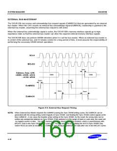
SYSTEM MANAGER
S3C4510B
SYSTEM CLOCK AND MUX BUS CONTROL REGISTER
CLOCK CONTROL REGISTER (CLKCON)
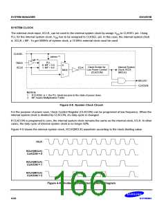
There is a clock control register in the System Manager. This control register is used to divide the internal system
clock, so the slower clock than the system clock can be made by clock dividing value. In this register, ROM bank
5 address/data MUX. enable control function is included.
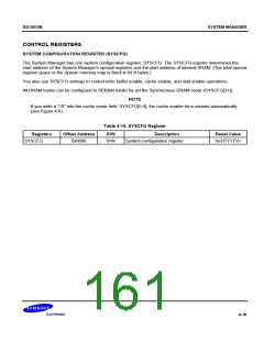
Table 4-17. CLKCON Register
Registers
CLKCON
Offset Address
R/W
Description
Clock control register
Reset Value
0x3000
R/W
0x00000000
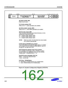
Table 4-18. CLKCON Register Description
Bit Number
Bit Name
Description
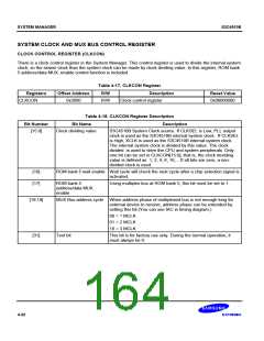
[15:0]
Clock dividing value
S3C4510B System Clock source. If CLKSEL is Low, PLL output
clock is used as the S3C4510B internal system clock. If CLKSEL
is High, XCLK is used as the S3C4510B internal system clock.
The internal system clock is divided by this value. The clock
divided is used to drive the CPU and system peripherals. Only
one bit can be set in CLKCON[15:0], that is, the clock deviding
value is defined as 1, 2, 4, 8, 16,... If all bits are zero, a non-
divided clock is used.
[16]
[17]
ROM bank 5 wait enable Wait cycle will check the next cycle after a chip selection signal is
activated.
ROM bank 5
address/data MUX.
enable
Using multiplex bus at ROM bank 5, this bit must be set to 1.
[19:18]
MUX Bus address cycle When address phase of multiplexed bus is not enough long for
external device to receive, address phase can be extended by
setting this bit.(You can see tAC in timing diagram.)
00 = 1 MCLK
01 = 2 MCLK
10 = 3 MCLK
[31]
Test bit
This bit is for factory use only. During the normal operation, it
must always be 0.
4-22

 SAMSUNG [ SAMSUNG ]