S3C4510B
SYSTEM MANAGER
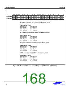
EXTERNAL I/O ACCESS CONTROL REGISTERS (EXTACON0/1)
The System Manager has four external I/O access control registers. These registers correspond to the up to four
external I/O banks that are supported by S3C4510B. Table 4-19 describes the two registers that are used to
control the timing of external I/O bank accesses.
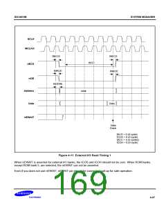
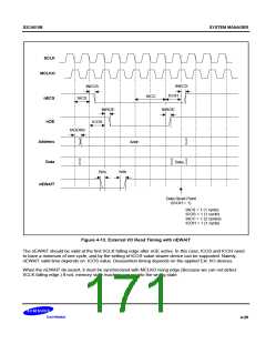
You can control external I/O access cycles using either a specified value or an external wait signal, nEWAIT. To
obtain access cycles that are longer than those possible with a specified value, you can delay the active time of
nOE or nWBE by tCOS value setting. After nOE or nWBE active, nEWAIT should be active previously at the first
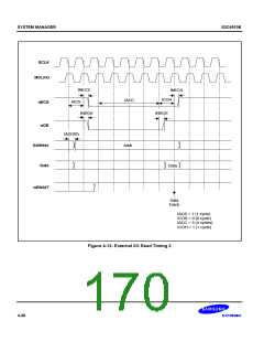
MCLK(SCLK) falling edge. In case of ROM bank 5, nRCS and nOE/nWBE signals are activated simultaneously,
that is, there is no control parameter as like tCOS. As a result, nEWAIT should be valid previously at the second
MCLK(SCLK) falling edge after nRCS active for the ROM bank 5.
EXTACON0 is used to set the access timings for external I/O banks 0 and 1. EXTACON1 is used to set the
external access timings for I/O banks 2 and 3.
NOTE
The base pointer for external I/O bank 0 is set in the REFEXTCON register(REFEXTCON register is in
DRAM control registers part).
Table 4-19. External I/O Access Control Register Description
Registers
EXTACON0
EXTACON1
Offset Address
0x3008
R/W
R/W
R/W
Description
Reset Value
0x00000000
0x00000000
External I/O access timing register 0
External I/O access timing register 1
0x300C
4-25

 SAMSUNG [ SAMSUNG ]