S3C4510B
SYSTEM MANAGER
Start Address Setting
The start address of the System Manager special register area is initialized to 3FFFF91H. (You can also set the
start address to an arbitrary value by writing the address, 3FF0000H.) When you have set the start address of the
special register area, the register addresses are automatically defined as the start address plus the register’s
offset.
Assume for example, that a reset initialize the start address to 3FF0000H. The offset address of the ROMCON
register is 3014H. Therefore, the physical address for ROMCON is 3FF0000H + 3014h = 3FF3014H. If you then
modified the start address of the special register area to 3000000H, the new address for the ROMCON register
would be 3003014H.
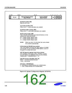
Cache Disable/Enable
To enable or disable the cache, you set the cache enable (CE) bit of the SYSCFG register to "1" or "0",
respectively Because cache memory does not have an auto-flush feature, you must be careful to verify the
coherency of data whenever you re-enable the cache. You must also carefully check any changes that the DMA
controller may make to data stored in memory.
(Usually, the memory area that is allocated to DMA access operations must be non-cachable.)
The internal 8-Kbyte SRAM can be used as a cache area. To configure this area, you use the cache mode bits,
SYSCFG[5:4]. If you do not need to use the entire 8-Kbyte area as cache, you can use the remaining area as
internal SRAM. This area is accessed using the address of the base pointer in the internal SRAM field.
Write Buffer Disable/Enable
The S3C4510B has four programmable write buffer registers that are used to improve the speed of memory write
operations. When you enable a write buffer, the CPU writes data into the write buffer, instead of an external
memory location. This saves the cycle that would normally be required to complete the external memory write
operation. The four write buffers also enhance the performance of the ARM7TDMI core’s store operations.
To maintain data coherency between the cache and external memory, the S3C4510B uses a write-through policy.
An internal 4-level write buffer compensates for performance degradation caused by write-throughs.
(For more information, read Chapter 5.)
4-21

 SAMSUNG [ SAMSUNG ]