SYSTEM MANAGER
SYSTEM CLOCK
S3C4510B
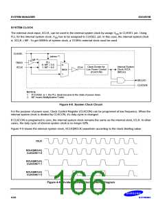
The external clock input, XCLK, can be used to the internal system clock by assign VDD to CLKSEL pin. Using
PLL for the internal system clock, VSS has to be assigned to CLKSEL pin. In this case, the internal system clock
is XCLK ´ MF. To get 50MHz of system clock, a 10 MHz external clock must be used.
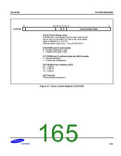
CLKSEL
pdown (1)
MF (2)
PLL
TMOD
XCLK
0: MF = 5.0
1: MF = 6.6
0
Clock Divider for
Low Power Control
(CLKCON)
Internal System
Clock SCLK
(MCLK)
ICLK
MUX
1
MCLKO
CLKOEN
NOTES:
1. If CLKSEL is 1, the PLL block became to the state of power down.
2. MF means Multiplication Factor.
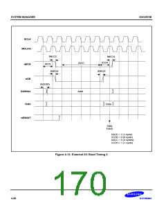
Figure 4-8. System Clock Circuit
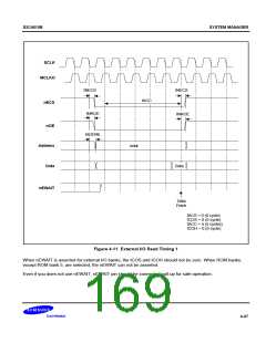
For the purpose of power save, Clock Control Register (CLKCON) can be programed at low frequency. When the
internal system clock is divided by CLKCON, it's duty-cycle is changed.
If CLKCON is programed to zero, the internal system clock remains the same as the internal clock, ICLK. In other
cases, the duty cycle of internal system clock is no longer 50%.
Figure 4-9 shows the internal system clock, SCLK(MCLK) waveform according to the clock dividing value.
ICLK
SCLK(MCLK)
CLKCON = 0
SCLK(MCLK)
CLKCON = 1
SCLK(MCLK)
CLKCON = 2
Figure 4-9. Divided System Clocks Timing Diagram
4-24

 SAMSUNG [ SAMSUNG ]