SYSTEM MANAGER
S3C4510B
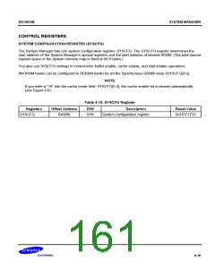
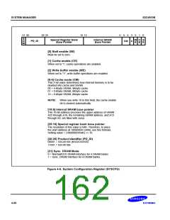
31 30
26 25
16 15
6
5
4
3
2
1
0
S
Special Register Bank
Base Pointer
Internal SRAM
Base Pointer
W C S
E E E
PD_ID
D
CM
0
M
[0] Stall enable (SE)
Must be set to zero.
[1] Cache enable (CE)
When set to '1', cache operations are enabled.
[2] Write buffer enable (WE)
When set to "1", write buffer operations are enabled.
[5:4] Cache mode (CM)
This 2-bit value determines how internal memory is to be
devided into cache and SRAM.
00 = 4-Kbyte SRAM, 4Kbyte cache
01 = 0-Kbyte SRAM, 8Kbyte cache
10 = 8-Kbyte SRAM, 0Kbyte cache
NOTE:
When you write 10 to this field, the cache enable
bit is cleared automatically.
[15:6] Internal SRAM base pointer
This 10-bit address becomes the upper address of SRAM.
A25 through A16, the remaining SRAM address, and A15
through A0, are filled with zeros.
[25:16] Special register bank base pointer
The resolution of this value is 64K. Therefore, to place
the start address at 1800000H (24M), use this formula:
Setting value = (1800000H/64K) << 16.
[30:26] Product Identifier (PD_ID)
00001 = S3C4510X (KS32C50100)
11001 = S3C4510B
[31] Sync. DRAM Mode
0 = Normal/EDO DRAM interface for 4 DRAM banks
1 = Sync. DRAM interface for 4 DRAM banks.
Figure 4-6. System Configuration Register (SYSCFG)
4-20

 SAMSUNG [ SAMSUNG ]