PRODUCT OVERVIEW
S3C4510B
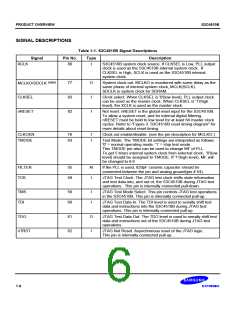
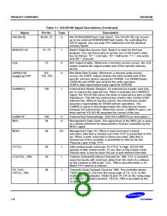
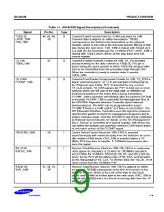
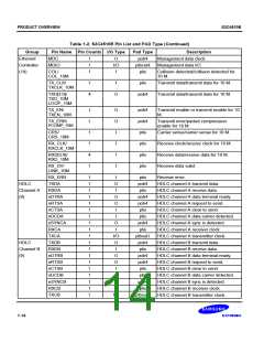
Table 1-1. S3C4510B Signal Descriptions (Continued)
Signal
Pin No.
Type
Description
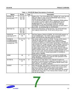
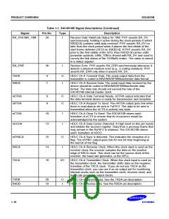
RX_DV/LINK_10M
29
I
Receive Data Valid/Link Status for 10M. PHY asserts RX_DV
synchronously, holding it active during the clock periods in which
RXD[3:0] contains valid data received. PHY asserts RX_DV no
later than the clock period when it places the first nibble of the
start frame delimiter (SFD) on RXD[3:0]. If PHY asserts RX_DV
prior to the first nibble of the SFD, then RXD[3:0] carries valid
preamble symbols. LINK_10M is shared with RX_DV and used to
convey the link status of the 10-Mbit/s endec. The value is stored
in a status register.
RX_ERR
36
I
Receive Error. PHY asserts RX_ERR synchronously whenever it
detects a physical medium error (e.g., a coding violation). PHY
asserts RX_ERR only when it asserts RX_DV.
TXDA
RXDA
9
7
O
I
HDLC Ch-A Transmit Data. The serial output data from the
transmitter is coded in NRZ/NRZI/FM/Manchester data format.
HDLC Ch-A Receive Data. The serial input data received by the
device should be coded in NRZ/NRZI/FM/Manchester data
format. The data rate should not exceed the rate of the
S3C4510B internal master clock.
nDTRA
nRTSA
6
8
O
O
HDLC Ch-A Data Terminal Ready. nDTRA output indicates that
the data terminal device is ready for transmission and reception.
HDLC Ch-A Request To Send. The nRTSA output goes low when
there is exist data to be sent in TxFIFO. The data to be sent is
transmitted when the nCTS is active(Low) state.
nCTSA
nDCDA
10
13
I
I
HDLC Ch-A Clear To Send. The S3C4510B stores each
transition of nCTS to ensure that its occurrence would be
acknowledged by the system.
HDLC Ch-A Data Carrier Detected. A High level on this pin resets
and inhibits the receiver register. Data from a previous frame that
may remain in the RxFIFO is retained. The S3C4510B stores
each transition of nDCD.
nSYNCA
RXCA
15
14
O
I
HDLC Ch-A Sync is detected. This indicates the reception of a
flag. The nSYNC output goes low for one bit time beginning at
the last bit of the flag.
HDLC Ch-A Receiver Clock. When this clock input is used as the
receiver clock, the receiver samples the data on the positive
edge of RXCA clock. This clock can be the source clock of the
receiver, the baud rate generator, or the DPLL.
TXCA
16
I/O
HDLC Ch-A Transmitter Clock. When this clock input is used as
the transmitter clock, the transmitter shifts data on the negative
transition of the TXCA clock . If you do not use TXCA as the
transmitter clock, you can use it as an output pin for monitoring
internal clocks such as the transmitter clock, receiver clock, and
baud rate generator output clocks.
TXDB
RXDB
20
18
O
I
HDLC Ch-B transmit data. See the TXDA pin description.
HDLC Ch-B receive data. See the RXDA pin description.
1-10

 SAMSUNG [ SAMSUNG ]