PRODUCT OVERVIEW
S3C4510B
SIGNAL DESCRIPTIONS
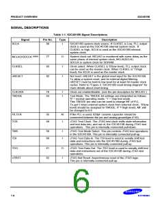
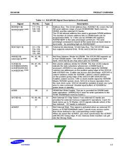
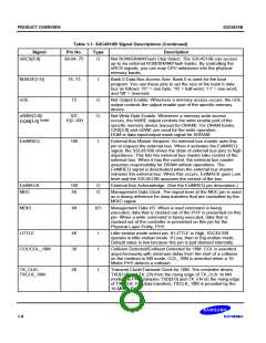
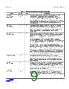
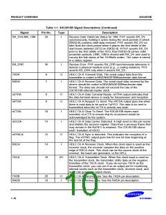
Table 1-1. S3C4510B Signal Descriptions
Signal
Pin No.
Type
Description
XCLK
80
I
S3C4510B system clock source. If CLKSEL is Low, PLL output
clock is used as the S3C4510B internal system clock. If
CLKSEL is High, XCLK is used as the S3C4510B internal
system clock.
MCLKO/SDCLK (note)
CLKSEL
77
83
82
O
I
System clock out. MCLKO is monitored with some delay as the
same phase of internal system clock, MCLK(SCLK).
SDCLK is system clock for SDRAM.
Clock select. When CLKSEL is '0'(low level), PLL output clock
can be used as the master clock. When CLKSEL is '1'(high
level), the XCLK is used as the master clock.
nRESET
I
Not reset. nRESET is the global reset input for the S3C4510B.
To allow a system reset, and for internal digital filtering,
nRESET must be held to low level for at least 64 master clock
cycles. Refer to "Figure 3. S3C4510B reset timing diagram" for
more details about reset timing.
CLKOEN
TMODE
76
63
I
I
Clock out enable/disable. (see the pin description for MCLKO.)
Test Mode. The TMODE bit settings are interpreted as follows:
'0' = normal operating mode, '1' = chip test mode.
This TMODE pin also can be used to change MF of PLL.
To get 5 times internal system clock from external clock, '0'(low
level) should be assigned to TMODE. If '1'(high level), MF will
be changed to 6.6
FILTER
TCK
55
58
AI
I
If the PLL is used, 820pF ceramic capacitor should be
connected between the pin and analog ground(pin # 54).
JTAG Test Clock. The JTAG test clock shifts state information
and test data into, and out of, the S3C4510B during JTAG test
operations. This pin is internally connected pull-down.
TMS
TDI
59
60
I
I
JTAG Test Mode Select. This pin controls JTAG test operations
in the S3C4510B. This pin is internally connected pull-up.
JTAG Test Data In. The TDI level is used to serially shift test
data and instructions into the S3C4510B during JTAG test
operations. This pin is internally connected pull-up.
TDO
61
62
O
I
JTAG Test Data Out. The TDO level is used to serially shift test
data and instructions out of the S3C4510B during JTAG test
operations.
nTRST
JTAG Not Reset. Asynchronous reset of the JTAG logic.
This pin is internally connected pull-up.
1-6

 SAMSUNG [ SAMSUNG ]