S3C4510B
PRODUCT OVERVIEW
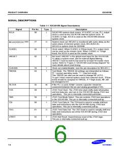
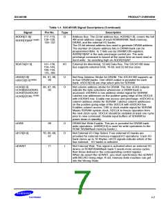
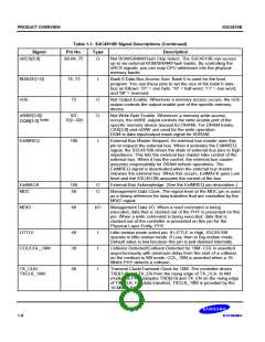
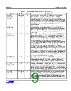
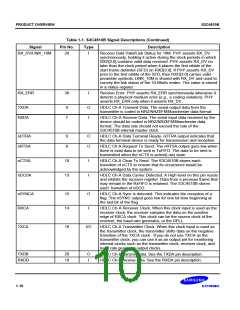
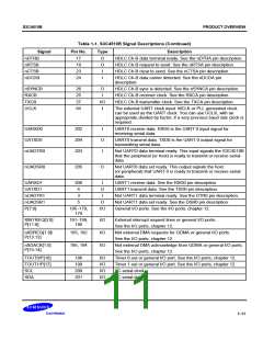
Table 1-1. S3C4510B Signal Descriptions (Continued)
Signal
Pin No.
Type
Description
ADDR[21:0]/
ADDR[10]/AP (note)
117–110,
129–120,
135–132
O
Address Bus. The 22-bit address bus, ADDR[21:0], covers the full
4M word address range of each ROM/SRAM, flash memory,
DRAM, and the external I/O banks.
The 23-bit internal address bus used to generate DRAM address.
The number of column address bits in DRAM bank can be
programmed 8bits to 11bits use by DRAMCON registers.
ADDR[10]/AP is the auto precharge control pin. The auto
precharge command is issued at the same time as burst read or
burst write by asserting high on ADDR[10]/AP.
XDATA[31:0]
141–136,
154–144,
166–159,
175–169
I/O
External (bi-directional, 32-bit) Data Bus. The S3C4510B data
bus supports external 8-bit, 16-bit, and 32-bit bus sizes.
nRAS[3:0]/
94, 91, 90,
89
O
O
Not Row Address Strobe for DRAM. The S3C4510B supports up
to four DRAM banks. One nRAS output is provided for each
bank. nSDCS[3:0] are chip select pins for SDRAM.
nSDCS[3:0] (note)
nCAS[3:0]
98, 97, 96,
95
Not column address strobe for DRAM. The four nCAS outputs
indicate the byte selections whenenver a DRAM bank is
accessed. nSDRAS is row address strobe signal for SDRAM.
Latches row addresses on the positive going edge of the SDCLK
with nSDRAS low. Enable row access and precharge. nSDCAS is
column address strobe for SDRAM. Latches column addresses
on the positive going edge of the SDCLK with nSDCAS low.
Enables column access. CKE is clock enable signal for SDRAM.
Masks SDRAM system clock, SDCLK to freeze operation from
the next clock cycle. SDCLK should be enabled at least one cycle
prior to new command. Disable input buffers of SDRAM for
power down in standby.
nCAS[0]/nSDRAS
nCAS[1]/nSDCAS
nCAS[2]/CKE (note)
nDWE
99
O
O
DRAM Not Write Enable. This pin is provided for DRAM bank
write operations. (nWBE[3:0] is used for write operations to the
ROM/ SRAM/flash memory banks.) .
nECS[3:0]
70, 69, 68,
67
Not External I/O Chip Select. Four external I/O banks are
provided for external memory-mapped I/O operations. Each I/O
bank stores up to 16 Kbytes. nECS signals indicate which of the
four external I/O banks is selected.
nEWAIT
71
I
Not External Wait. This signal is activated when an external I/O
device or ROM/SRAM/flash bank 5 needs more access cycles
than those defined in the corresponding control register.
When de-assert the nEWAIT, you must synchronize the nEWAIT
with MCLKO rising edge. If not, memory state machine can get
into the Wrong State.
1-7

 SAMSUNG [ SAMSUNG ]