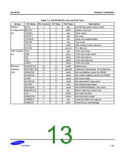
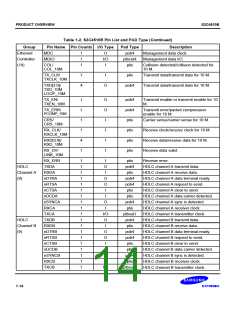
S3C4510B
PRODUCT OVERVIEW
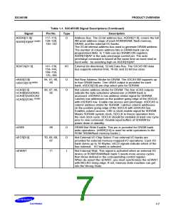
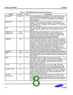
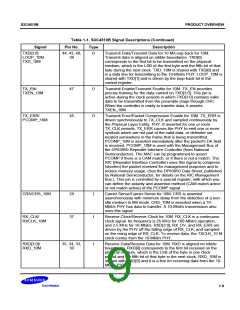
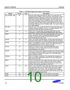
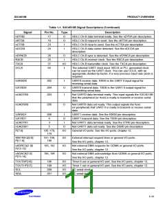
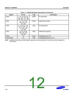
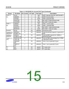
Table 1-1. S3C4510B Signal Descriptions (Continued)
Signal
Pin No.
17
Type
Description
nDTRB
nRTSB
nCTSB
nDCDB
O
O
I
HDLC Ch-B data terminal ready. See the nDTRA pin description.
HDLC Ch-B request to send. See the nRTSA pin description.
HDLC Ch-B clear to send. See the nCTSA pin description.
19
23
24
I
HDLC Ch-B data carrier detected. See the nDCDA pin
description.
nSYNCB
RXCB
TXCB
26
25
27
64
O
I
HDLC Ch-B sync is detected. See the nSYNCA pin description.
HDLC Ch-B receiver clock. See the RXCA pin description.
HDLC Ch-B transmitter clock. See the TXCA pin description.
I/O
I
UCLK
The external UART clock input. MCLK or PLL generated clock
can be used as the UART clock. You can use UCLK, with an
appropriate divided by factor, if a very precious baud rate clock is
required.
UARXD0
UATXD0
nUADTR0
202
204
203
I
O
I
UART0 receive data. RXD0 is the UART 0 input signal for
receiving serial data.
UART0 transmit data. TXD0 is the UART 0 output signal for
transmitting serial data.
Not UART0 data terminal ready. This input signals the S3C4510B
that the peripheral (or host) is ready to transmit or receive serial
data.
nUADSR0
205
O
Not UART0 data set ready. This output signals the host
(or peripheral) that UART 0 is ready to transmit or receive serial
data.
UARXD1
UATXD1
nUADTR1
nUADSR1
P[7:0]
206
4
I
O
I
UART1 receive data. See the RXD0 pin description.
UART1 transmit data. See the TXD0 pin description.
Not UART1 data terminal ready. See the DTR0 pin description.
Not UART1 data set ready. See the DSR0 pin description.
General I/O ports. See the I/O ports, chapter 12.
3
5
O
I/O
185–179,
176
XINTREQ[3:0]
P[11:8]
191–189,
186
I/O
I/O
I/O
External interrupt request lines or general I/O ports.
See the I/O ports, chapter 12.
nXDREQ[1:0]/
P[13:12]
193, 192
Not external DMA requests for GDMA or general I/O ports.
See the I/O ports, chapter 12.
nXDACK[1:0]
P[15:14]
195, 194
Not external DMA acknowledge from GDMA or general I/O ports.
See the I/O ports, chapter 12.
TOUT0/P[16]
TOUT1/P[17]
SCL
196
199
200
201
I/O
I/O
I/O
I/O
Timer 0 out or general I/O port. See the I/O ports, chapter 12.
Timer 1 out or general I/O port. See the I/O ports, chapter 12.
I2C serial clock.
SDA
I2C serial data.
1-11

 SAMSUNG [ SAMSUNG ]