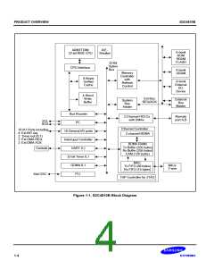
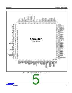
PRODUCT OVERVIEW
S3C4510B
Table 1-1. S3C4510B Signal Descriptions (Continued)
Signal
Pin No.
Type
Description
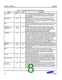
nRCS[5:0]
88-84, 75
O
Not ROM/SRAM/Flash Chip Select. The S3C4510B can access
up to six external ROM/SRAM/Flash banks. By controlling the
nRCS signals, you can map CPU addresses into the physical
memory banks.
B0SIZE[1:0]
nOE
74, 73
72
I
Bank 0 Data Bus Access Size. Bank 0 is used for the boot
program. You use these pins to set the size of the bank 0 data
bus as follows: '01' = one byte, '10' = half-word, '11' = one word,
and '00' = reserved.
O
O
Not Output Enable. Whenever a memory access occurs, the nOE
output controls the output enable port of the specific memory
device.
nWBE[3:0]/
DQM[3:0] (note)
107,
102–100
Not Write Byte Enable. Whenever a memory write access
occurs, the nWBE output controls the write enable port of the
specific memory device (except for DRAM). For DRAM banks,
CAS[3:0] and nDWE are used for the write operation.
DQM is data input/output mask signal for SDRAM.
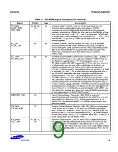
ExtMREQ
108
I
External Bus Master Request. An external bus master uses this
pin to request the external bus. When it activates the ExtMREQ
signal, the S3C4510B drives the state of external bus pins to high
impedance. This lets the external bus master take control of the
external bus. When it has the control, the external bus master
assumes responsibility for DRAM refresh operations. The
ExtMREQ signal is deactivated when the external bus master
releases the external bus. When this occurs, ExtMACK goes Low
level and the S3C4510B assumes the control of the bus.
ExtMACK
MDC
109
50
O
O
External Bus Acknowledge. (See the ExtMREQ pin description.)
Management Data Clock. The signal level at the MDC pin is used
as a timing reference for data transfers that are controlled by the
MDIO signal.
MDIO
48
I/O
Management Data I/O. When a read command is being
executed, data that is clocked out of the PHY is presented on this
pin. When a write command is being executed, data that is
clocked out of the controller is presented on this pin for the
Physical Layer Entity, PHY.
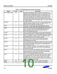
LITTLE
49
38
I
I
Little endian mode select pin. If LITTLE is High, S3C4510B
operate in little endian mode. If Low, then in Big endian mode.
Default value is low because this pin is pull-downed internally.
COL/COL_10M
Collision Detected/Collision Detected for 10M. COL is asserted
asynchronously with minimum delay from the start of a collision
on the medium in MII mode. COL_10M is asserted when a 10-
Mbit/s PHY detects a collision.
TX_CLK/
TXCLK_10M
46
I
Transmit Clock/Transmit Clock for 10M. The controller drives
TXD[3:0] and TX_EN from the rising edge of TX_CLK. In MII
mode, the PHY samples TXD[3:0] and TX_EN on the rising edge
of TX_CLK. For data transfers, TXCLK_10M is provided by the
10-Mbit/s PHY.
1-8

 SAMSUNG [ SAMSUNG ]