S3C4510B
PRODUCT OVERVIEW
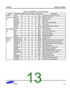
Table 1-2. S3C4510B Pin List and PAD Type
Group
Pin Name Pin Counts I/O Type
Pad Type
ptic
Description
System
XCLK
1
1
1
1
1
1
1
1
1
1
1
1
1
22
32
4
4
1
4
1
6
2
1
4
1
1
I
O
I
S3C4510B system source clock.
System clock out.
Configuration MCLKO
pob4
ptic
(8)
CLKSEL
nRESET
CLKOEN
TMODE
LITTLE
Clock select.
I
ptis
Not reset
I
ptic
Clock out enable/disable.
Test mode.
I
ptic
I
pticd
pia_bb
ptic
Little endian mode select pin
PLL filter pin
FILTER
I
TAP Control TCK
I
JTAG test clock.
(5)
TMS
I
pticu
pticu
ptot2
pticu
ptot6
ptbsut6
ptot4
ptot4
ptot4
ptot4
ptic
JTAG test mode select.
JTAG test data in.
TDI
I
TDO
O
I
JTAG test data out.
nTRST
JTAG not reset.
Memory
Interface
(83)
ADDR[21:0]
XDATA[31:0]
nRAS[3:0]
nCAS[3:0]
nDWE
O
I/O
O
O
O
O
I
Address bus.
External, bi-directional, 32-bit data bus.
Not row address strobe for DRAM.
Not column address strobe for DRAM.
Not write enable
nECS[3:0]
nEWAIT
nRCS[5:0]
B0SIZE[1:0]
nOE
Not external I/O chip select.
Not external wait signal.
Not ROM/SRAM/flash chip select.
Bank 0 data bus access size.
Not output enable.
O
I
ptot4
ptic
O
O
I
ptot4
ptot4
ptic
nWBE[3:0]
ExtMREQ
ExtMACK
Not write byte enable.
External master bus request.
External bus acknowledge.
O
pob1
1-13

 SAMSUNG [ SAMSUNG ]