MS18R1622(4/8)DH0
(16Mx18)*2(4/8)pcs SO-RIMM™ based on 288Mb D-die, 32s banks,16K/32ms Refresh, 2.5V
Key Timing Parameters/Part Numbers
Overview
The following table lists the frequency and latency bins
available for SO-RIMM modules.
The SO-RIMM™ module is a general purpose high-perfor-
mance memory subsystem suitable for a broad range of
applications including networking systemsnetworking
systems, digital con sumer systems, mobile "Thin and light"
PCs, and other applications where high bandwidth and low
latency are required.
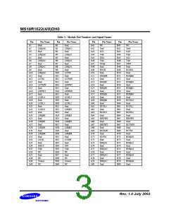
Table 1: Part Number by Freq. & Latency
Speed
I/O
Freq.
t
rac
The SO-RIMM module consists of 288Mb RDRAM
devices.These are extremely high speed CMOS DRAMs
organized as 16M words by 18 bits. The use of Rambus
Signaling Level(RSL) technology permits up to 1066MHz
transfer rates while using conventional system and board
design technologies. RDRAM devices are capable of
sustained data transfers up to at 0.94ns per two bytes (7.5ns
per 16 bytes)
Organization
Part Number
(Row
Access
Time) ns
Bin
(MHz)
-CT9
-CN9
1066
1066
32P
32
MS18R1622DH0-CT9
MS18R1622DH0-CN9
MS18R1622DH0-CM9
MS18R1622DH0-CM8
MS18R1622DH0-CK8
MS18R1624DH0-CT9
MS18R1624DH0-CN9
MS18R1624DH0-CM9
MS18R1624DH0-CM8
MS18R1624DH0-CK8
MS18R1628DH0-CT9
MS18R1628DH0-CN9
MS18R1628DH0-CM9
MS18R1628DH0-CM8
MS18R1628DH0-CK8
32M x 18
-CM9 1066
35
-CM8
-CK8
-CT9
-CN9
800
800
40
45
The RDRAM Architecture enables the highest sustained
bandwidth for multiple, simultaneous, randomly addressed,
memory transactions. The seperate control and data buses
with independent row and column control yield high bus
efficiency. The RDRAM device’s thirty-two bank architec-
ture supports up to four simultaneous transactions per
device.
1066
1066
32P
32
64M x 18
-CM9 1066
35
-CM8
-CK8
-CT9
-CN9
800
800
40
45
1066
1066
32P
32
Features
128M x 18
-CM9 1066
35
♦ High speed of 1066MHz and 800MHz per pin
♦ 160 edge connector pads with 0.65mm pad spacing
♦ Maximum module PCB size : 67.6mm x 31.25mm x
1.00mm (2.66” x 1.23” x 0.039”)
-CM8
-CK8
800
800
40
45
♦ Each RDRAM device has 32 banks, for a total of
256,128,64 banks on each 288MB,144MB,72MB module
respectively
♦ Gold plated edge connector pad contacts
♦ Serial Presence Detect(SPD) support
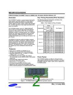
Form Factor
The SO-RIMM modules are offered in 160-pad 0.65mm
edge connector pad pitch form factor suitable for 160 contact
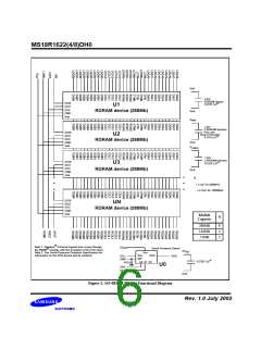
SO-RIMM connectors. Figure 1 below, shows a eight device
SO-RIMM module.
♦ Operates from a 2.5 volt supply (± 5%)
♦ Low power and powerdown self refresh modes
♦ Sperate Row and Column buses for heigher efficiency
♦ WBGA lead free package for SO-RIMM Module(92 balls)
Note: On double sided modules, RDRAM devices are also installed on bottom side of PCB.
Figure 1: SO-RIMM Module shown with heat spreader removed
Rev. 1.0 July 2002
Page 1

 SAMSUNG [ SAMSUNG ]